Repository: mhyousefi/MIPS-pipeline-processor
Branch: master
Commit: 0410b0fc0bc9
Files: 30
Total size: 58.4 KB
Directory structure:
gitextract_pppgpag3/

├── .gitignore
├── README.md
├── alteraDE2SimulationFiles/
│   ├── 7segConv.v
│   └── DE2_TOP.V
├── defines.v
├── instructions/
│   ├── example_source_code.txt
│   └── rearrange_instructions.py
├── modules/
│   ├── ALU.v
│   ├── adder.v
│   ├── controlUnit/
│   │   ├── conditionChecker.v
│   │   └── controller.v
│   ├── hazard_forwarding/
│   │   ├── forwarding.v
│   │   └── hazardDetection.v
│   ├── memoryModules/
│   │   ├── dataMem.v
│   │   ├── instructionMem.v
│   │   └── regFile.v
│   ├── mux.v
│   ├── pipeRegisters/
│   │   ├── EXE2MEM.v
│   │   ├── ID2EXE.v
│   │   ├── IF2ID.v
│   │   └── MEM2WB.v
│   ├── pipeStages/
│   │   ├── EXEStage.v
│   │   ├── IDStage.v
│   │   ├── IFStage.v
│   │   ├── MEMStage.v
│   │   └── WBStage.v
│   ├── register.v
│   └── signExtend.v
├── testbench.v
└── topLevelCircuit.v
================================================
FILE CONTENTS
================================================
================================================
FILE: .gitignore
================================================
*.csv
*.mpf
*.qpf
*.qsf
*.v.bak
*.wlf
*.cr.mti
.DS_Store
configs/
db/
incremental_db/
output_files/
simulation/
work/
instructions/ready_instructions.txt
================================================
FILE: README.md
================================================
# MIPS-pipeline-processor
Thanks for visiting this repository!
Developed during the Fall 2017 Computer Architecture Laboratory course at the University of Tehran,
this project is an implementation of a pipelined MIPS processor featuring hazard detection as well as forwarding.
This implementation is based on a limited ISA, the details for which are present in `docs/MIPS_ISA.png`.
This code is synthesizable and can be run on an FPGA. We used Altera DE2 units for testing purposes. The implemtation has been verified using a relatively complex test program (found in `instructions/example_source_code.txt`).
## Getting Started
Download or clone the project, write your machine code to run (there already exists a default test program in the instruction memory),
compile the Verilog files and and run testbench.v in a Verilog simulation environment such as ModelSim from Mentor Graphics.
### Instruction format
Instructions should be provided to the instruction memory in reset time. We avoided the `readmemb` and `readmemh` functions to
keep the code synthesizable. The instruction memory cells are 8 bits long, whereas each instruction is 32 bits long.
Therefore, each instruction takes up four memory cells, as shown bellow.
For example, an add instruction: `10000000001000000000000000001010` or `Addi r1,r0,10` will need to be given as
```
instMem[0] <= 8'b10000000;
instMem[1] <= 8'b00100000;
instMem[2] <= 8'b00000000;
instMem[3] <= 8'b00001010;
```
### Converting your raw machine codes
A python script is provided under the `instructions/rearrange_instructions.py` directory which simply takes your
machine code (in a specified format) and converts it to the format illustrated above.
### Enable/disable forwarding
An instance of the top-level circuit is taken in `testbench.v`.
The inputs of the `MIPS_Processor` include `clk`, `rst`, and `forwarding_EN`.
Forwarding will be enabled if `forwarding_EN` is set to 1, and disabled otherwise.
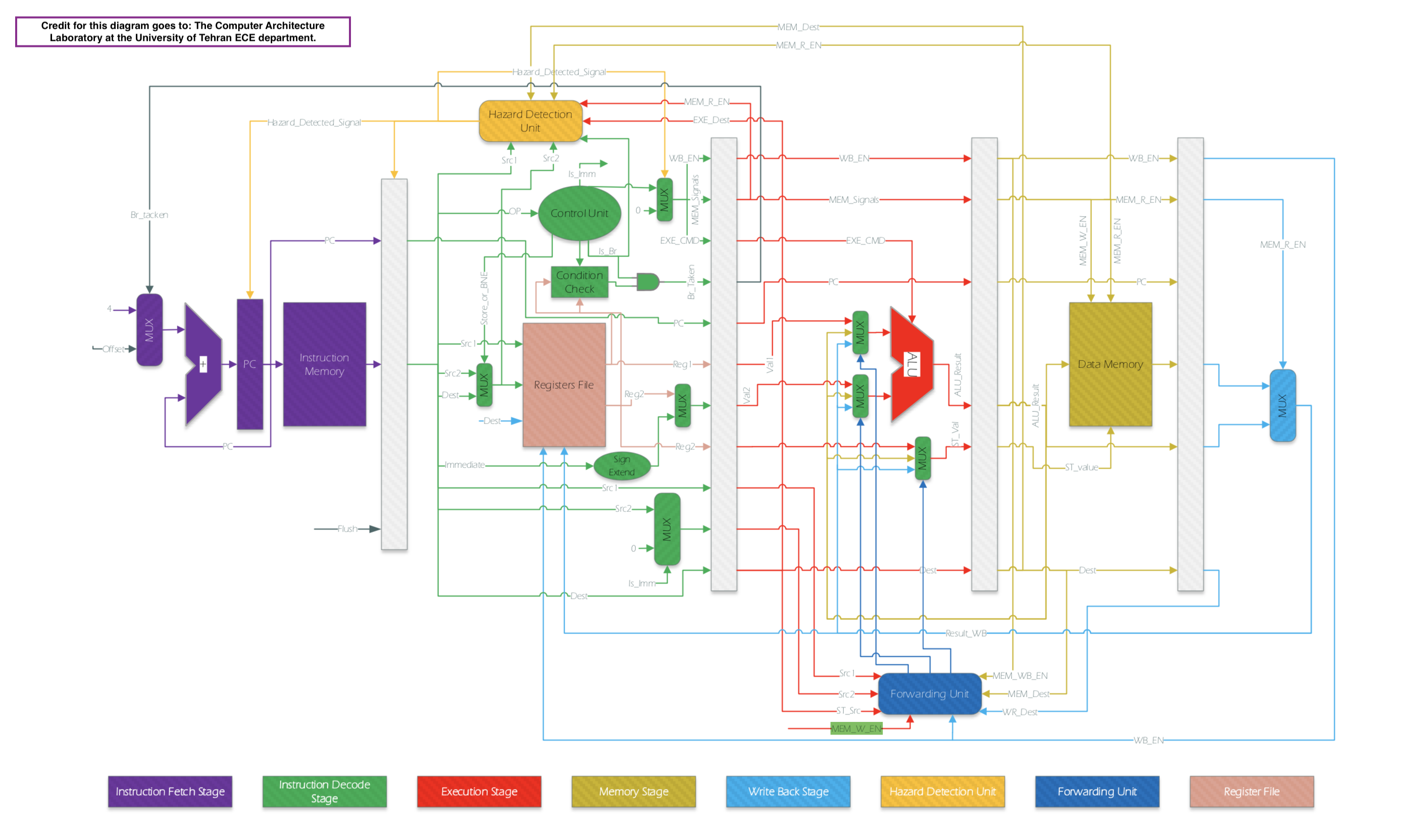
## Under the hood
There are five pipeline stages:
1. Instruction Fetch
2. Instruction Decode
3. Execution
4. Memory
5. Write Back
### Modular design
All modules are organized under the `modules` directory.
The top level description can be found under `topLevelCircuit.v`. It contains a **modular design** of the processor and
encompasses five pipe stages and four pipe registers, the description for which are present under `modules/pipeStages` and
`modules/pipeRegisters` respectively. The register file, the hazard detection and the forwarding units are also instantiated
in `topLevelCircuit.v`. Pipe stages are made of and encapsulate other supporting modules.
### Constants
`defines.v` contains project-wide constants for **opcodes**, **execution commands**, and **branch condition commands**.
It also contains constants for wire widths and memory specifications. You can change memory size values to suit your needs.
### Wire naming convention
To maintain conformity, most wire names follow the format {wire description}_{wire stage}, where the second part describes
the stage where the wire is located. For example, `MEM_W_EN_ID` is the memory write enable signal present in the instruction decode stage.
## Contributions
Contributions are welcomed, both general improvements as well as new features such as a more realistic memory heirarchy or branch prediction. However, please follow the coding styles and the naming convention. Another useful contribution would be more comprehensive testing and verification and bug report.
================================================
FILE: alteraDE2SimulationFiles/7segConv.v
================================================
module sevenSegConv (num, out1, out2);
input [31:0] num;
output [6:0] out1, out2;
wire [31:0] numLower = num / 10;
wire [31:0] numUpper = num % 10;
assign out1 = (numLower == 32'd0) ? 7'b1000000:
(numLower == 32'd1) ? 7'b1001111:
(numLower == 32'd2) ? 7'b0100100:
(numLower == 32'd3) ? 7'b0110000:
(numLower == 32'd4) ? 7'b0011001:
(numLower == 32'd5) ? 7'b0010010:
(numLower == 32'd6) ? 7'b0000010:
(numLower == 32'd7) ? 7'b1111000:
(numLower == 32'd8) ? 7'b0000000:
(numLower == 32'd9) ? 7'b0010000: 7'b1111111;
assign out2 = (numUpper == 32'd0) ? 7'b1000000:
(numUpper == 32'd1) ? 7'b1001111:
(numUpper == 32'd2) ? 7'b0100100:
(numUpper == 32'd3) ? 7'b0110000:
(numUpper == 32'd4) ? 7'b0011001:
(numUpper == 32'd5) ? 7'b0010010:
(numUpper == 32'd6) ? 7'b0000010:
(numUpper == 32'd7) ? 7'b1111000:
(numUpper == 32'd8) ? 7'b0000000:
(numUpper == 32'd9) ? 7'b0010000: 7'b1111111;
endmodule // sevenSegConv
================================================
FILE: alteraDE2SimulationFiles/DE2_TOP.V
================================================
module DE2_TOP
(
//////////////////// Clock Input ////////////////////
CLOCK_27, // 27 MHz
CLOCK_50, // 50 MHz
EXT_CLOCK, // External Clock
//////////////////// Push Button ////////////////////
KEY, // Pushbutton[3:0]
//////////////////// DPDT Switch ////////////////////
SW, // Toggle Switch[17:0]
//////////////////// 7-SEG Dispaly ////////////////////
HEX0, // Seven Segment Digit 0
HEX1, // Seven Segment Digit 1
HEX2, // Seven Segment Digit 2
HEX3, // Seven Segment Digit 3
HEX4, // Seven Segment Digit 4
HEX5, // Seven Segment Digit 5
HEX6, // Seven Segment Digit 6
HEX7, // Seven Segment Digit 7
//////////////////////// LED ////////////////////////
LEDG, // LED Green[8:0]
LEDR, // LED Red[17:0]
//////////////////////// UART ////////////////////////
UART_TXD, // UART Transmitter
UART_RXD, // UART Receiver
//////////////////////// IRDA ////////////////////////
// IRDA_TXD, // IRDA Transmitter
// IRDA_RXD, // IRDA Receiver
///////////////////// SDRAM Interface ////////////////
DRAM_DQ, // SDRAM Data bus 16 Bits
DRAM_ADDR, // SDRAM Address bus 12 Bits
DRAM_LDQM, // SDRAM Low-byte Data Mask
DRAM_UDQM, // SDRAM High-byte Data Mask
DRAM_WE_N, // SDRAM Write Enable
DRAM_CAS_N, // SDRAM Column Address Strobe
DRAM_RAS_N, // SDRAM Row Address Strobe
DRAM_CS_N, // SDRAM Chip Select
DRAM_BA_0, // SDRAM Bank Address 0
DRAM_BA_1, // SDRAM Bank Address 0
DRAM_CLK, // SDRAM Clock
DRAM_CKE, // SDRAM Clock Enable
//////////////////// Flash Interface ////////////////
FL_DQ, // FLASH Data bus 8 Bits
FL_ADDR, // FLASH Address bus 22 Bits
FL_WE_N, // FLASH Write Enable
FL_RST_N, // FLASH Reset
FL_OE_N, // FLASH Output Enable
FL_CE_N, // FLASH Chip Enable
//////////////////// SRAM Interface ////////////////
SRAM_DQ, // SRAM Data bus 16 Bits
SRAM_ADDR, // SRAM Address bus 18 Bits
SRAM_UB_N, // SRAM High-byte Data Mask
SRAM_LB_N, // SRAM Low-byte Data Mask
SRAM_WE_N, // SRAM Write Enable
SRAM_CE_N, // SRAM Chip Enable
SRAM_OE_N, // SRAM Output Enable
//////////////////// ISP1362 Interface ////////////////
OTG_DATA, // ISP1362 Data bus 16 Bits
OTG_ADDR, // ISP1362 Address 2 Bits
OTG_CS_N, // ISP1362 Chip Select
OTG_RD_N, // ISP1362 Write
OTG_WR_N, // ISP1362 Read
OTG_RST_N, // ISP1362 Reset
OTG_FSPEED, // USB Full Speed, 0 = Enable, Z = Disable
OTG_LSPEED, // USB Low Speed, 0 = Enable, Z = Disable
OTG_INT0, // ISP1362 Interrupt 0
OTG_INT1, // ISP1362 Interrupt 1
OTG_DREQ0, // ISP1362 DMA Request 0
OTG_DREQ1, // ISP1362 DMA Request 1
OTG_DACK0_N, // ISP1362 DMA Acknowledge 0
OTG_DACK1_N, // ISP1362 DMA Acknowledge 1
//////////////////// LCD Module 16X2 ////////////////
LCD_ON, // LCD Power ON/OFF
LCD_BLON, // LCD Back Light ON/OFF
LCD_RW, // LCD Read/Write Select, 0 = Write, 1 = Read
LCD_EN, // LCD Enable
LCD_RS, // LCD Command/Data Select, 0 = Command, 1 = Data
LCD_DATA, // LCD Data bus 8 bits
//////////////////// SD_Card Interface ////////////////
//SD_DAT, // SD Card Data
SD_WP_N, // SD Write protect
SD_CMD, // SD Card Command Signal
SD_CLK, // SD Card Clock
//////////////////// USB JTAG link ////////////////////
TDI, // CPLD -> FPGA (data in)
TCK, // CPLD -> FPGA (clk)
TCS, // CPLD -> FPGA (CS)
TDO, // FPGA -> CPLD (data out)
//////////////////// I2C ////////////////////////////
I2C_SDAT, // I2C Data
I2C_SCLK, // I2C Clock
//////////////////// PS2 ////////////////////////////
PS2_DAT, // PS2 Data
PS2_CLK, // PS2 Clock
//////////////////// VGA ////////////////////////////
VGA_CLK, // VGA Clock
VGA_HS, // VGA H_SYNC
VGA_VS, // VGA V_SYNC
VGA_BLANK, // VGA BLANK
VGA_SYNC, // VGA SYNC
VGA_R, // VGA Red[9:0]
VGA_G, // VGA Green[9:0]
VGA_B, // VGA Blue[9:0]
//////////// Ethernet Interface ////////////////////////
ENET_DATA, // DM9000A DATA bus 16Bits
ENET_CMD, // DM9000A Command/Data Select, 0 = Command, 1 = Data
ENET_CS_N, // DM9000A Chip Select
ENET_WR_N, // DM9000A Write
ENET_RD_N, // DM9000A Read
ENET_RST_N, // DM9000A Reset
ENET_INT, // DM9000A Interrupt
ENET_CLK, // DM9000A Clock 25 MHz
//////////////// Audio CODEC ////////////////////////
AUD_ADCLRCK, // Audio CODEC ADC LR Clock
AUD_ADCDAT, // Audio CODEC ADC Data
AUD_DACLRCK, // Audio CODEC DAC LR Clock
AUD_DACDAT, // Audio CODEC DAC Data
AUD_BCLK, // Audio CODEC Bit-Stream Clock
AUD_XCK, // Audio CODEC Chip Clock
//////////////// TV Decoder ////////////////////////
TD_DATA, // TV Decoder Data bus 8 bits
TD_HS, // TV Decoder H_SYNC
TD_VS, // TV Decoder V_SYNC
TD_RESET, // TV Decoder Reset
TD_CLK27, // TV Decoder 27MHz CLK
//////////////////// GPIO ////////////////////////////
GPIO_0, // GPIO Connection 0
GPIO_1 // GPIO Connection 1
);
//////////////////////// Clock Input ////////////////////////
input CLOCK_27; // 27 MHz
input CLOCK_50; // 50 MHz
input EXT_CLOCK; // External Clock
//////////////////////// Push Button ////////////////////////
input [3:0] KEY; // Pushbutton[3:0]
//////////////////////// DPDT Switch ////////////////////////
input [17:0] SW; // Toggle Switch[17:0]
//////////////////////// 7-SEG Dispaly ////////////////////////
output [6:0] HEX0; // Seven Segment Digit 0
output [6:0] HEX1; // Seven Segment Digit 1
output [6:0] HEX2; // Seven Segment Digit 2
output [6:0] HEX3; // Seven Segment Digit 3
output [6:0] HEX4; // Seven Segment Digit 4
output [6:0] HEX5; // Seven Segment Digit 5
output [6:0] HEX6; // Seven Segment Digit 6
output [6:0] HEX7; // Seven Segment Digit 7
//////////////////////////// LED ////////////////////////////
output [8:0] LEDG; // LED Green[8:0]
output [17:0] LEDR; // LED Red[17:0]
//////////////////////////// UART ////////////////////////////
output UART_TXD; // UART Transmitter
input UART_RXD; // UART Receiver
//////////////////////////// IRDA ////////////////////////////
//output IRDA_TXD; // IRDA Transmitter
//input IRDA_RXD; // IRDA Receiver
/////////////////////// SDRAM Interface ////////////////////////
inout [15:0] DRAM_DQ; // SDRAM Data bus 16 Bits
output [11:0] DRAM_ADDR; // SDRAM Address bus 12 Bits
output DRAM_LDQM; // SDRAM Low-byte Data Mask
output DRAM_UDQM; // SDRAM High-byte Data Mask
output DRAM_WE_N; // SDRAM Write Enable
output DRAM_CAS_N; // SDRAM Column Address Strobe
output DRAM_RAS_N; // SDRAM Row Address Strobe
output DRAM_CS_N; // SDRAM Chip Select
output DRAM_BA_0; // SDRAM Bank Address 0
output DRAM_BA_1; // SDRAM Bank Address 0
output DRAM_CLK; // SDRAM Clock
output DRAM_CKE; // SDRAM Clock Enable
//////////////////////// Flash Interface ////////////////////////
inout [7:0] FL_DQ; // FLASH Data bus 8 Bits
output [21:0] FL_ADDR; // FLASH Address bus 22 Bits
output FL_WE_N; // FLASH Write Enable
output FL_RST_N; // FLASH Reset
output FL_OE_N; // FLASH Output Enable
output FL_CE_N; // FLASH Chip Enable
//////////////////////// SRAM Interface ////////////////////////
inout [15:0] SRAM_DQ; // SRAM Data bus 16 Bits
output [17:0] SRAM_ADDR; // SRAM Address bus 18 Bits
output SRAM_UB_N; // SRAM High-byte Data Mask
output SRAM_LB_N; // SRAM Low-byte Data Mask
output SRAM_WE_N; // SRAM Write Enable
output SRAM_CE_N; // SRAM Chip Enable
output SRAM_OE_N; // SRAM Output Enable
//////////////////// ISP1362 Interface ////////////////////////
inout [15:0] OTG_DATA; // ISP1362 Data bus 16 Bits
output [1:0] OTG_ADDR; // ISP1362 Address 2 Bits
output OTG_CS_N; // ISP1362 Chip Select
output OTG_RD_N; // ISP1362 Write
output OTG_WR_N; // ISP1362 Read
output OTG_RST_N; // ISP1362 Reset
output OTG_FSPEED; // USB Full Speed, 0 = Enable, Z = Disable
output OTG_LSPEED; // USB Low Speed, 0 = Enable, Z = Disable
input OTG_INT0; // ISP1362 Interrupt 0
input OTG_INT1; // ISP1362 Interrupt 1
input OTG_DREQ0; // ISP1362 DMA Request 0
input OTG_DREQ1; // ISP1362 DMA Request 1
output OTG_DACK0_N; // ISP1362 DMA Acknowledge 0
output OTG_DACK1_N; // ISP1362 DMA Acknowledge 1
//////////////////// LCD Module 16X2 ////////////////////////////
inout [7:0] LCD_DATA; // LCD Data bus 8 bits
output LCD_ON; // LCD Power ON/OFF
output LCD_BLON; // LCD Back Light ON/OFF
output LCD_RW; // LCD Read/Write Select, 0 = Write, 1 = Read
output LCD_EN; // LCD Enable
output LCD_RS; // LCD Command/Data Select, 0 = Command, 1 = Data
//////////////////// SD Card Interface ////////////////////////
//inout [3:0] SD_DAT; // SD Card Data
input SD_WP_N; // SD write protect
inout SD_CMD; // SD Card Command Signal
output SD_CLK; // SD Card Clock
//////////////////////// I2C ////////////////////////////////
inout I2C_SDAT; // I2C Data
output I2C_SCLK; // I2C Clock
//////////////////////// PS2 ////////////////////////////////
input PS2_DAT; // PS2 Data
input PS2_CLK; // PS2 Clock
//////////////////// USB JTAG link ////////////////////////////
input TDI; // CPLD -> FPGA (data in)
input TCK; // CPLD -> FPGA (clk)
input TCS; // CPLD -> FPGA (CS)
output TDO; // FPGA -> CPLD (data out)
//////////////////////// VGA ////////////////////////////
output VGA_CLK; // VGA Clock
output VGA_HS; // VGA H_SYNC
output VGA_VS; // VGA V_SYNC
output VGA_BLANK; // VGA BLANK
output VGA_SYNC; // VGA SYNC
output [9:0] VGA_R; // VGA Red[9:0]
output [9:0] VGA_G; // VGA Green[9:0]
output [9:0] VGA_B; // VGA Blue[9:0]
//////////////// Ethernet Interface ////////////////////////////
inout [15:0] ENET_DATA; // DM9000A DATA bus 16Bits
output ENET_CMD; // DM9000A Command/Data Select, 0 = Command, 1 = Data
output ENET_CS_N; // DM9000A Chip Select
output ENET_WR_N; // DM9000A Write
output ENET_RD_N; // DM9000A Read
output ENET_RST_N; // DM9000A Reset
input ENET_INT; // DM9000A Interrupt
output ENET_CLK; // DM9000A Clock 25 MHz
//////////////////// Audio CODEC ////////////////////////////
inout AUD_ADCLRCK; // Audio CODEC ADC LR Clock
input AUD_ADCDAT; // Audio CODEC ADC Data
inout AUD_DACLRCK; // Audio CODEC DAC LR Clock
output AUD_DACDAT; // Audio CODEC DAC Data
inout AUD_BCLK; // Audio CODEC Bit-Stream Clock
output AUD_XCK; // Audio CODEC Chip Clock
//////////////////// TV Devoder ////////////////////////////
input [7:0] TD_DATA; // TV Decoder Data bus 8 bits
input TD_HS; // TV Decoder H_SYNC
input TD_VS; // TV Decoder V_SYNC
output TD_RESET; // TV Decoder Reset
input TD_CLK27; // TV Decoder 27MHz CLK
//////////////////////// GPIO ////////////////////////////////
inout [35:0] GPIO_0; // GPIO Connection 0
inout [35:0] GPIO_1; // GPIO Connection 1
wire clock = CLOCK_50;
wire [31:0] PC_IF, PC_ID, PC_EXE, PC_MEM;
wire [31:0] inst_IF, inst_ID;
wire [31:0] reg1_ID, reg2_ID, ST_value_EXE, ST_value_EXE2MEM, ST_value_MEM;
wire [31:0] val1_ID, val1_EXE;
wire [31:0] val2_ID, val2_EXE;
wire [31:0] ALURes_EXE, ALURes_MEM, ALURes_WB;
wire [31:0] dataMem_out_MEM, dataMem_out_WB;
wire [31:0] WB_result;
wire [4:0] dest_EXE, dest_MEM, dest_WB; // dest_ID = instruction[25:21] thus nothing declared
wire [4:0] src1_ID, src2_regFile_ID, src2_forw_ID, src2_forw_EXE, src1_forw_EXE;
wire [3:0] EXE_CMD_ID, EXE_CMD_EXE;
wire [1:0] val1_sel, val2_sel, ST_val_sel;
wire [1:0] branch_comm;
wire Br_Taken_ID, IF_Flush, Br_Taken_EXE;
wire MEM_R_EN_ID, MEM_R_EN_EXE, MEM_R_EN_MEM, MEM_R_EN_WB;
wire MEM_W_EN_ID, MEM_W_EN_EXE, MEM_W_EN_MEM;
wire WB_EN_ID, WB_EN_EXE, WB_EN_MEM, WB_EN_WB;
wire hazard_detected, is_imm, ST_or_BNE;
regFile regFile(
// INPUTS
.clk(clock),
.rst(SW[0]),
.src1(src1_ID),
.src2(src2_regFile_ID),
.dest(dest_WB),
.writeVal(WB_result),
.writeEn(WB_EN_WB),
// OUTPUTS
.reg1(reg1_ID),
.reg2(reg2_ID)
);
hazard_detection hazard (
// INPUTS
.forward_EN(SW[1]),
.is_imm(is_imm),
.ST_or_BNE(ST_or_BNE),
.src1_ID(src1_ID),
.src2_ID(src2_regFile_ID),
.dest_EXE(dest_EXE),
.dest_MEM(dest_MEM),
.WB_EN_EXE(WB_EN_EXE),
.WB_EN_MEM(WB_EN_MEM),
.MEM_R_EN_EXE(MEM_R_EN_EXE),
// OUTPUTS
.branch_comm(branch_comm),
.hazard_detected(hazard_detected)
);
forwarding_EXE forwrding_EXE (
.src1_EXE(src1_forw_EXE),
.src2_EXE(src2_forw_EXE),
.ST_src_EXE(dest_EXE),
.dest_MEM(dest_MEM),
.dest_WB(dest_WB),
.WB_EN_MEM(WB_EN_MEM),
.WB_EN_WB(WB_EN_WB),
.val1_sel(val1_sel),
.val2_sel(val2_sel),
.ST_val_sel(ST_val_sel)
);
//###########################
//##### PIPLINE STAGES ######
//###########################
IFStage IFStage (
// INPUTS
.clk(clock),
.rst(SW[0]),
.freeze(hazard_detected),
.brTaken(Br_Taken_ID),
.brOffset(val2_ID),
// OUTPUTS
.instruction(inst_IF),
.PC(PC_IF)
);
IDStage IDStage (
// INPUTS
.clk(clock),
.rst(SW[0]),
.hazard_detected_in(hazard_detected),
.instruction(inst_ID),
.reg1(reg1_ID),
.reg2(reg2_ID),
// OUTPUTS
.src1(src1_ID),
.src2_reg_file(src2_regFile_ID),
.src2_forw(src2_forw_ID),
.val1(val1_ID),
.val2(val2_ID),
.brTaken(Br_Taken_ID),
.EXE_CMD(EXE_CMD_ID),
.MEM_R_EN(MEM_R_EN_ID),
.MEM_W_EN(MEM_W_EN_ID),
.WB_EN(WB_EN_ID),
.is_imm_out(is_imm),
.ST_or_BNE_out(ST_or_BNE),
.branch_comm(branch_comm)
);
EXEStage EXEStage (
// INPUTS
.clk(clock),
.EXE_CMD(EXE_CMD_EXE),
.val1_sel(val1_sel),
.val2_sel(val2_sel),
.ST_val_sel(ST_val_sel),
.val1(val1_EXE),
.val2(val2_EXE),
.ALU_res_MEM(ALURes_MEM),
.result_WB(WB_result),
.ST_value_in(ST_value_EXE),
// OUTPUTS
.ALUResult(ALURes_EXE),
.ST_value_out(ST_value_EXE2MEM)
);
MEMStage MEMStage (
// INPUTS
.clk(clock),
.rst(SW[0]),
.MEM_R_EN(MEM_R_EN_MEM),
.MEM_W_EN(MEM_W_EN_MEM),
.ALU_res(ALURes_MEM),
.ST_value(ST_value_MEM),
// OUTPUTS
.dataMem_out(dataMem_out_MEM)
);
WBStage WBStage (
// INPUTS
.MEM_R_EN(MEM_R_EN_WB),
.memData(dataMem_out_WB),
.aluRes(ALURes_WB),
// OUTPUTS
.WB_res(WB_result)
);
//###########################
//#### PIPLINE REISTERS #####
//###########################
IF2ID IF2IDReg (
// INPUTS
.clk(clock),
.rst(SW[0]),
.flush(IF_Flush),
.freeze(hazard_detected),
.PCIn(PC_IF),
.instructionIn(inst_IF),
// OUTPUTS
.PC(PC_ID),
.instruction(inst_ID)
);
ID2EXE ID2EXEReg (
.clk(clock),
.rst(SW[0]),
// INPUTS
.destIn(inst_ID[25:21]),
.src1_in(src1_ID),
.src2_in(src2_forw_ID),
.reg2In(reg2_ID),
.val1In(val1_ID),
.val2In(val2_ID),
.PCIn(PC_ID),
.EXE_CMD_IN(EXE_CMD_ID),
.MEM_R_EN_IN(MEM_R_EN_ID),
.MEM_W_EN_IN(MEM_W_EN_ID),
.WB_EN_IN(WB_EN_ID),
.brTaken_in(Br_Taken_ID),
// OUTPUTS
.src1_out(src1_forw_EXE),
.src2_out(src2_forw_EXE),
.dest(dest_EXE),
.ST_value(ST_value_EXE),
.val1(val1_EXE),
.val2(val2_EXE),
.PC(PC_EXE),
.EXE_CMD(EXE_CMD_EXE),
.MEM_R_EN(MEM_R_EN_EXE),
.MEM_W_EN(MEM_W_EN_EXE),
.WB_EN(WB_EN_EXE),
.brTaken_out(Br_Taken_EXE)
);
EXE2MEM EXE2MEMReg (
.clk(clock),
.rst(SW[0]),
// INPUTS
.WB_EN_IN(WB_EN_EXE),
.MEM_R_EN_IN(MEM_R_EN_EXE),
.MEM_W_EN_IN(MEM_W_EN_EXE),
.PCIn(PC_EXE),
.ALUResIn(ALURes_EXE),
.STValIn(ST_value_EXE2MEM),
.destIn(dest_EXE),
// OUTPUTS
.WB_EN(WB_EN_MEM),
.MEM_R_EN(MEM_R_EN_MEM),
.MEM_W_EN(MEM_W_EN_MEM),
.PC(PC_MEM),
.ALURes(ALURes_MEM),
.STVal(ST_value_MEM),
.dest(dest_MEM)
);
MEM2WB MEM2WB(
.clk(clock),
.rst(SW[0]),
// INPUTS
.WB_EN_IN(WB_EN_MEM),
.MEM_R_EN_IN(MEM_R_EN_MEM),
.ALUResIn(ALURes_MEM),
.memReadValIn(dataMem_out_MEM),
.destIn(dest_MEM),
// OUTPUTS
.WB_EN(WB_EN_WB),
.MEM_R_EN(MEM_R_EN_WB),
.ALURes(ALURes_WB),
.memReadVal(dataMem_out_WB),
.dest(dest_WB)
);
assign IF_Flush = Br_Taken_ID;
endmodule
================================================
FILE: defines.v
================================================
// Wire widths
`define WORD_LEN 32
`define REG_FILE_ADDR_LEN 5
`define EXE_CMD_LEN 4
`define FORW_SEL_LEN 2
`define OP_CODE_LEN 6
// Memory constants
`define DATA_MEM_SIZE 1024
`define INSTR_MEM_SIZE 1024
`define REG_FILE_SIZE 32
`define MEM_CELL_SIZE 8
// To be used inside controller.v
`define OP_NOP 6'b000000
`define OP_ADD 6'b000001
`define OP_SUB 6'b000011
`define OP_AND 6'b000101
`define OP_OR 6'b000110
`define OP_NOR 6'b000111
`define OP_XOR 6'b001000
`define OP_SLA 6'b001001
`define OP_SLL 6'b001010
`define OP_SRA 6'b001011
`define OP_SRL 6'b001100
`define OP_ADDI 6'b100000
`define OP_SUBI 6'b100001
`define OP_LD 6'b100100
`define OP_ST 6'b100101
`define OP_BEZ 6'b101000
`define OP_BNE 6'b101001
`define OP_JMP 6'b101010
// To be used in side ALU
`define EXE_ADD 4'b0000
`define EXE_SUB 4'b0010
`define EXE_AND 4'b0100
`define EXE_OR 4'b0101
`define EXE_NOR 4'b0110
`define EXE_XOR 4'b0111
`define EXE_SLA 4'b1000
`define EXE_SLL 4'b1000
`define EXE_SRA 4'b1001
`define EXE_SRL 4'b1010
`define EXE_NO_OPERATION 4'b1111 // for NOP, BEZ, BNQ, JMP
// To be used in conditionChecker
`define COND_JUMP 2'b10
`define COND_BEZ 2'b11
`define COND_BNE 2'b01
`define COND_NOTHING 2'b00
================================================
FILE: instructions/example_source_code.txt
================================================
10000000001000000000000000001010; Addi r1,r0,10 *** (1 begins) performing basic arithmetic operations
00000100010000000000100000000000; Add r2,r0,r1 ***
00001100011000000000100000000000; sub r3,r0,r1 ***
00010100100000100001100000000000; And r4,r2,r3 ***
10000100101000000000001000110100; Subi r5,r0,564 ***
00011000101001010001100000000000; or r5,r5,r3 ***
00011100110001010000000000000000; nor r6,r5,r0 ***
00100000000001010000100000000000; xor r0,r5,r1 ***
00100000111001010000100000000000; xor r7,r5,r1 ***
00100100111001000001000000000000; sla r7,r4,r2 ***
00101001000000110001000000000000; sll r8,r3,r2 ***
00101101001001100001000000000000; sra r9,r6,r2 ***
00110001010001100001000000000000; srl r10,r6,r2 *** (1 ends)
10000000001000000000010000000000; Addi r1,r0,1024 *** (2 begins) exchanging some data with the memory
10010100010000010000000000000000; st r2,r1,0 ***
10010001011000010000000000000000; ld r11,r1,0 ***
10010100011000010000000000000100; st r3,r1,4 ***
10010100100000010000000000001000; st r4,r1,8 ***
10010100101000010000000000001100; st r5,r1,12 ***
10010100110000010000000000010000; st r6,r1,16 ***
10010100111000010000000000010100; st r7,r1,20 ***
10010101000000010000000000011000; st r8,r1,24 ***
10010101001000010000000000011100; st r9,r1,28 ***
10010101010000010000000000100000; st r10,r1,32 ***
10010101011000010000000000100100; st r11,r1,36 *** (2 ends)
10000000001000000000000000000011; Addi r1,r0,3 *** =====> BUBBLE SORT BEGINS
10000000100000000000010000000000; Addi r4,r0,1024 ***
10000000010000000000000000000000; Addi r2,r0,0 ***
10000000011000000000000000000001; Addi r3,r0,1 *** (outer loop begins)
10000001001000000000000000000010; Addi r9,r0,2 *** (inner loop begins)
00101001000000110100100000000000; sll r8,r3,r9 *** (3 begins) loading two consecutive numbers to compare
00000101000001000100000000000000; Add r8,r4,r8 ***
10010000101010000000000000000000; ld r5,r8,0 ***
10010000110010001111111111111100; ld r6,r8,-4 ***
00001101001001010011000000000000; sub r9,r5,r6 ***
10000001010000001000000000000000; Addi r10,r0,0x8000 ***
10000001011000000000000000010000; Addi r11,r0,16 ***
00101001010010100101100000000000; sll r10,r10,r11 ***
00010101001010010101000000000000; And r9,r9,r10 *** (3 ends)
10100000000010010000000000000010; Bez r9,2 *** (4 begins) swapping the two loaded numbers if needed
10010100101010001111111111111100; st r5,r8,-4 ***
10010100110010000000000000000000; st r6,r8,0 *** (4 ends)
10000000011000110000000000000001; Addi r3,r3,1 *** R3++
10100100011000011111111111110001; BNE r3,r1,-15 *** (inner loop ends)
10000000010000100000000000000001; Addi r2,r2,1 *** R2++
10100100010000011111111111101110; BNE r2,r1,-18 *** (outer loop ends) =====> BUBBLE SORT ENDS
10000000001000000000010000000000; Addi r1,r0,1024 *** (5 begins) storing some register inside memory
10010000010000010000000000000000; ld r2,r1,0 ***
10010000011000010000000000000100; ld r3,r1,4 ***
10010000100000010000000000001000; ld r4,r1,8 ***
10010000101000010000000000001100; ld r5,r1,12 ***
10010000110000010000000000010000; ld r6,r1,16 ***
10010000111000010000000000010100; ld r7,r1,20 ***
10010001000000010000000000011000; ld r8,r1,24 ***
10010001001000010000000000011100; ld r9,r1,28 ***
10010001010000010000000000100000; ld r10,r1,32 ***
10010001011000010000000000100100; ld r11,r1,36 *** (5 ends)
10101000000000001111111111111111; JMP -1 *** will keep jumping to itself
================================================
FILE: instructions/rearrange_instructions.py
================================================
#!/usr/bin/env python
# -*- coding: utf-8 -*-
# Rearranging instructions from a source file to a format suitable for the always statement under instructionMem.v
# There is an example source code under this directory
# In drafting your own code, make sure you follow the ISA in this project
DESTINATION_FILE_NAME = "ready_instructions.txt"
INSTR_MEM_ARRAY_NAME = "instMem"
line_count = int(raw_input("Enter the number of instructions to rearrange: "))
source_file_name = raw_input("Enter the source file name: ")
instructions = []
with open(source_file_name, "r") as instr_file:
for i in range(line_count):
instructions.append(instr_file.readline()[:-1])
with open(DESTINATION_FILE_NAME, "w") as dest_file:
for i in range(len(instructions)):
instr = instructions[i]
dest_file.write(INSTR_MEM_ARRAY_NAME + "[" + str(i*4) + "] <= 8'b" + instr[0:8] + "; // ==> " + instr[34:] + "\n")
dest_file.write(INSTR_MEM_ARRAY_NAME + "[" + str(i*4+1) + "] <= 8'b" + instr[8:16] + ";\n")
dest_file.write(INSTR_MEM_ARRAY_NAME + "[" + str(i*4+2) + "] <= 8'b" + instr[16:24] + ";\n")
dest_file.write(INSTR_MEM_ARRAY_NAME + "[" + str(i*4+3) + "] <= 8'b" + instr[24:32] + ";\n\n")
print "💡💡💡 ==> instructions reformatted for instruction memory."
print "To run them, copy and paste the content of ready_instructions.txt under the reset if statement in the instructionMem.v always statement."
================================================
FILE: modules/ALU.v
================================================
`include "defines.v"
module ALU (val1, val2, EXE_CMD, aluOut);
input [`WORD_LEN-1:0] val1, val2;
input [`EXE_CMD_LEN-1:0] EXE_CMD;
output reg [`WORD_LEN-1:0] aluOut;
always @ ( * ) begin
case (EXE_CMD)
`EXE_ADD: aluOut <= val1 + val2;
`EXE_SUB: aluOut <= val1 - val2;
`EXE_AND: aluOut <= val1 & val2;
`EXE_OR: aluOut <= val1 | val2;
`EXE_NOR: aluOut <= ~(val1 | val2);
`EXE_XOR: aluOut <= val1 ^ val2;
`EXE_SLA: aluOut <= val1 << val2;
`EXE_SLL: aluOut <= val1 <<< val2;
`EXE_SRA: aluOut <= val1 >> val2;
`EXE_SRL: aluOut <= val1 >>> val2;
default: aluOut <= 0;
endcase
end
endmodule // ALU
================================================
FILE: modules/adder.v
================================================
`include "defines.v"
module adder (in1, in2, out);
input [`WORD_LEN-1:0] in1, in2;
output [`WORD_LEN-1:0] out;
assign out = in1 + in2;
endmodule // adder
================================================
FILE: modules/controlUnit/conditionChecker.v
================================================
`include "defines.v"
module conditionChecker (reg1, reg2, cuBranchComm, brCond);
input [`WORD_LEN-1: 0] reg1, reg2;
input [1:0] cuBranchComm;
output reg brCond;
always @ ( * ) begin
case (cuBranchComm)
`COND_JUMP: brCond <= 1;
`COND_BEZ: brCond <= (reg1 == 0) ? 1 : 0;
`COND_BNE: brCond <= (reg1 != reg2) ? 1 : 0;
default: brCond <= 0;
endcase
end
endmodule // conditionChecker
================================================
FILE: modules/controlUnit/controller.v
================================================
`include "defines.v"
module controller (opCode, branchEn, EXE_CMD, Branch_command, Is_Imm, ST_or_BNE, WB_EN, MEM_R_EN, MEM_W_EN, hazard_detected);
input hazard_detected;
input [`OP_CODE_LEN-1:0] opCode;
output reg branchEn;
output reg [`EXE_CMD_LEN-1:0] EXE_CMD;
output reg [1:0] Branch_command;
output reg Is_Imm, ST_or_BNE, WB_EN, MEM_R_EN, MEM_W_EN;
always @ ( * ) begin
if (hazard_detected == 0) begin
{branchEn, EXE_CMD, Branch_command, Is_Imm, ST_or_BNE, WB_EN, MEM_R_EN, MEM_W_EN} <= 0;
case (opCode)
// operations writing to the register file
`OP_ADD: begin EXE_CMD <= `EXE_ADD; WB_EN <= 1; end
`OP_SUB: begin EXE_CMD <= `EXE_SUB; WB_EN <= 1; end
`OP_AND: begin EXE_CMD <= `EXE_AND; WB_EN <= 1; end
`OP_OR: begin EXE_CMD <= `EXE_OR; WB_EN <= 1; end
`OP_NOR: begin EXE_CMD <= `EXE_NOR; WB_EN <= 1; end
`OP_XOR: begin EXE_CMD <= `EXE_XOR; WB_EN <= 1; end
`OP_SLA: begin EXE_CMD <= `EXE_SLA; WB_EN <= 1; end
`OP_SLL: begin EXE_CMD <= `EXE_SLL; WB_EN <= 1; end
`OP_SRA: begin EXE_CMD <= `EXE_SRA; WB_EN <= 1; end
`OP_SRL: begin EXE_CMD <= `EXE_SRL; WB_EN <= 1; end
// operations using an immediate value embedded in the instruction
`OP_ADDI: begin EXE_CMD <= `EXE_ADD; WB_EN <= 1; Is_Imm <= 1; end
`OP_SUBI: begin EXE_CMD <= `EXE_SUB; WB_EN <= 1; Is_Imm <= 1; end
// memory operations
`OP_LD: begin EXE_CMD <= `EXE_ADD; WB_EN <= 1; Is_Imm <= 1; ST_or_BNE <= 1; MEM_R_EN <= 1; end
`OP_ST: begin EXE_CMD <= `EXE_ADD; Is_Imm <= 1; MEM_W_EN <= 1; ST_or_BNE <= 1; end
// branch operations
`OP_BEZ: begin EXE_CMD <= `EXE_NO_OPERATION; Is_Imm <= 1; Branch_command <= `COND_BEZ; branchEn <= 1; end
`OP_BNE: begin EXE_CMD <= `EXE_NO_OPERATION; Is_Imm <= 1; Branch_command <= `COND_BNE; branchEn <= 1; ST_or_BNE <= 1; end
`OP_JMP: begin EXE_CMD <= `EXE_NO_OPERATION; Is_Imm <= 1; Branch_command <= `COND_JUMP; branchEn <= 1; end
default: {branchEn, EXE_CMD, Branch_command, Is_Imm, ST_or_BNE, WB_EN, MEM_R_EN, MEM_W_EN} <= 0;
endcase
end
else if (hazard_detected == 1) begin
// preventing any writes to the register file or the memory
{EXE_CMD, WB_EN, MEM_W_EN} <= 0;
end
end
endmodule // controller
================================================
FILE: modules/hazard_forwarding/forwarding.v
================================================
`include "defines.v"
module forwarding_EXE (src1_EXE, src2_EXE, ST_src_EXE, dest_MEM, dest_WB, WB_EN_MEM, WB_EN_WB, val1_sel, val2_sel, ST_val_sel);
input [`REG_FILE_ADDR_LEN-1:0] src1_EXE, src2_EXE, ST_src_EXE;
input [`REG_FILE_ADDR_LEN-1:0] dest_MEM, dest_WB;
input WB_EN_MEM, WB_EN_WB;
output reg [`FORW_SEL_LEN-1:0] val1_sel, val2_sel, ST_val_sel;
always @ ( * ) begin
// initializing sel signals to 0
// they will change to enable forwrding if needed.
{val1_sel, val2_sel, ST_val_sel} <= 0;
// determining forwarding control signal for store value (ST_val)
if (WB_EN_MEM && ST_src_EXE == dest_MEM) ST_val_sel <= 2'd1;
else if (WB_EN_WB && ST_src_EXE == dest_WB) ST_val_sel <= 2'd2;
// determining forwarding control signal for ALU val1
if (WB_EN_MEM && src1_EXE == dest_MEM) val1_sel <= 2'd1;
else if (WB_EN_WB && src1_EXE == dest_WB) val1_sel <= 2'd2;
// determining forwarding control signal for ALU val2
if (WB_EN_MEM && src2_EXE == dest_MEM) val2_sel <= 2'd1;
else if (WB_EN_WB && src2_EXE == dest_WB) val2_sel <= 2'd2;
end
endmodule // forwarding
================================================
FILE: modules/hazard_forwarding/hazardDetection.v
================================================
`include "defines.v"
module hazard_detection(forward_EN, is_imm, ST_or_BNE, src1_ID, src2_ID, dest_EXE, WB_EN_EXE, dest_MEM, WB_EN_MEM, MEM_R_EN_EXE, branch_comm, hazard_detected);
input [`REG_FILE_ADDR_LEN-1:0] src1_ID, src2_ID;
input [`REG_FILE_ADDR_LEN-1:0] dest_EXE, dest_MEM;
input [1:0] branch_comm;
input forward_EN, WB_EN_EXE, WB_EN_MEM, is_imm, ST_or_BNE, MEM_R_EN_EXE;
output hazard_detected;
wire src2_is_valid, exe_has_hazard, mem_has_hazard, hazard, instr_is_branch;
assign src2_is_valid = (~is_imm) || ST_or_BNE;
assign exe_has_hazard = WB_EN_EXE && (src1_ID == dest_EXE || (src2_is_valid && src2_ID == dest_EXE));
assign mem_has_hazard = WB_EN_MEM && (src1_ID == dest_MEM || (src2_is_valid && src2_ID == dest_MEM));
assign hazard = (exe_has_hazard || mem_has_hazard);
assign instr_is_branch = (branch_comm == `COND_BEZ || branch_comm == `COND_BNE);
assign hazard_detected = ~forward_EN ? hazard : (instr_is_branch && hazard) || (MEM_R_EN_EXE && mem_has_hazard);
endmodule // hazard_detection
================================================
FILE: modules/memoryModules/dataMem.v
================================================
`include "defines.v"
module dataMem (clk, rst, writeEn, readEn, address, dataIn, dataOut);
input clk, rst, readEn, writeEn;
input [`WORD_LEN-1:0] address, dataIn;
output [`WORD_LEN-1:0] dataOut;
integer i;
reg [`MEM_CELL_SIZE-1:0] dataMem [0:`DATA_MEM_SIZE-1];
wire [`WORD_LEN-1:0] base_address;
always @ (posedge clk) begin
if (rst)
for (i = 0; i < `DATA_MEM_SIZE; i = i + 1)
dataMem[i] <= 0;
else if (writeEn)
{dataMem[base_address], dataMem[base_address + 1], dataMem[base_address + 2], dataMem[base_address + 3]} <= dataIn;
end
assign base_address = ((address & 32'b11111111111111111111101111111111) >> 2) << 2;
assign dataOut = (address < 1024) ? 0 : {dataMem[base_address], dataMem[base_address + 1], dataMem[base_address + 2], dataMem[base_address + 3]};
endmodule // dataMem
================================================
FILE: modules/memoryModules/instructionMem.v
================================================
`include "defines.v"
module instructionMem (rst, addr, instruction);
input rst;
input [`WORD_LEN-1:0] addr;
output [`WORD_LEN-1:0] instruction;
wire [$clog2(`INSTR_MEM_SIZE)-1:0] address = addr[$clog2(`INSTR_MEM_SIZE)-1:0];
reg [`MEM_CELL_SIZE-1:0] instMem [0:`INSTR_MEM_SIZE-1];
always @ (*) begin
if (rst) begin
// No nop added in between instructions since there is a hazard detection unit
instMem[0] <= 8'b10000000; //-- Addi r1,r0,10
instMem[1] <= 8'b00100000;
instMem[2] <= 8'b00000000;
instMem[3] <= 8'b00001010;
instMem[4] <= 8'b00000100; //-- Add r2,r0,r1
instMem[5] <= 8'b01000000;
instMem[6] <= 8'b00001000;
instMem[7] <= 8'b00000000;
instMem[8] <= 8'b00001100; //-- sub r3,r0,r1
instMem[9] <= 8'b01100000;
instMem[10] <= 8'b00001000;
instMem[11] <= 8'b00000000;
instMem[12] <= 8'b00010100; //-- And r4,r2,r3
instMem[13] <= 8'b10000010;
instMem[14] <= 8'b00011000;
instMem[15] <= 8'b00000000;
instMem[16] <= 8'b10000100; //-- Subi r5,r0,564
instMem[17] <= 8'b10100000;
instMem[18] <= 8'b00000010;
instMem[19] <= 8'b00110100;
instMem[20] <= 8'b00011000; //-- or r5,r5,r3
instMem[21] <= 8'b10100101;
instMem[22] <= 8'b00011000;
instMem[23] <= 8'b00000000;
instMem[24] <= 8'b00011100; //-- nor r6,r5,r0
instMem[25] <= 8'b11000101;
instMem[26] <= 8'b00000000;
instMem[27] <= 8'b00000000;
instMem[28] <= 8'b00100000; //-- xor r0,r5,r1
instMem[29] <= 8'b00000101;
instMem[30] <= 8'b00001000;
instMem[31] <= 8'b00000000;
instMem[32] <= 8'b00100000; //-- xor r7,r5,r0
instMem[33] <= 8'b11100101;
instMem[34] <= 8'b00001000;
instMem[35] <= 8'b00000000;
instMem[36] <= 8'b00100100; //-- sla r7,r4,r2
instMem[37] <= 8'b11100100;
instMem[38] <= 8'b00010000;
instMem[39] <= 8'b00000000;
instMem[40] <= 8'b00101001; //-- sll r8,r3,r2
instMem[41] <= 8'b00000011;
instMem[42] <= 8'b00010000;
instMem[43] <= 8'b00000000;
instMem[44] <= 8'b00101101; //-- sra r9,r6,r2
instMem[45] <= 8'b00100110;
instMem[46] <= 8'b00010000;
instMem[47] <= 8'b00000000;
instMem[48] <= 8'b00110001; //-- srl r10,r6,r2
instMem[49] <= 8'b01000110;
instMem[50] <= 8'b00010000;
instMem[51] <= 8'b00000000;
instMem[52] <= 8'b10000000; //-- Addi r1,r0,1024
instMem[53] <= 8'b00100000;
instMem[54] <= 8'b00000100;
instMem[55] <= 8'b00000000;
instMem[56] <= 8'b10010100; //-- st r2,r1,0
instMem[57] <= 8'b01000001;
instMem[58] <= 8'b00000000;
instMem[59] <= 8'b00000000;
instMem[60] <= 8'b10010001; //-- ld r11,r1,0
instMem[61] <= 8'b01100001;
instMem[62] <= 8'b00000000;
instMem[63] <= 8'b00000000;
instMem[64] <= 8'b10010100; //-- st r3,r1,4
instMem[65] <= 8'b01100001;
instMem[66] <= 8'b00000000;
instMem[67] <= 8'b00000100;
instMem[68] <= 8'b10010100; //-- st r4,r1,8
instMem[69] <= 8'b10000001;
instMem[70] <= 8'b00000000;
instMem[71] <= 8'b00001000;
instMem[72] <= 8'b10010100; //-- st r5,r1,12
instMem[73] <= 8'b10100001;
instMem[74] <= 8'b00000000;
instMem[75] <= 8'b00001100;
instMem[76] <= 8'b10010100; //-- st r6,r1,16
instMem[77] <= 8'b11000001;
instMem[78] <= 8'b00000000;
instMem[79] <= 8'b00010000;
instMem[80] <= 8'b10010100; //-- st r7,r1,20
instMem[81] <= 8'b11100001;
instMem[82] <= 8'b00000000;
instMem[83] <= 8'b00010100;
instMem[84] <= 8'b10010101; //-- st r8,r1,24
instMem[85] <= 8'b00000001;
instMem[86] <= 8'b00000000;
instMem[87] <= 8'b00011000;
instMem[88] <= 8'b10010101; //-- st r9,r1,28
instMem[89] <= 8'b00100001;
instMem[90] <= 8'b00000000;
instMem[91] <= 8'b00011100;
instMem[92] <= 8'b10010101; //-- st r10,r1,32
instMem[93] <= 8'b01000001;
instMem[94] <= 8'b00000000;
instMem[95] <= 8'b00100000;
instMem[96] <= 8'b10010101; //-- st r11,r1,36
instMem[97] <= 8'b01100001;
instMem[98] <= 8'b00000000;
instMem[99] <= 8'b00100100;
instMem[100] <= 8'b10000000; //-- Addi r1,r0,3
instMem[101] <= 8'b00100000;
instMem[102] <= 8'b00000000;
instMem[103] <= 8'b00000011;
instMem[104] <= 8'b10000000; //-- Addi r4,r0,1024
instMem[105] <= 8'b10000000;
instMem[106] <= 8'b00000100;
instMem[107] <= 8'b00000000;
instMem[108] <= 8'b10000000; //-- Addi r2,r0,0
instMem[109] <= 8'b01000000;
instMem[110] <= 8'b00000000;
instMem[111] <= 8'b00000000;
instMem[112] <= 8'b10000000; //-- Addi r3,r0,1
instMem[113] <= 8'b01100000;
instMem[114] <= 8'b00000000;
instMem[115] <= 8'b00000001;
instMem[116] <= 8'b10000001; //-- Addi r9,r0,2
instMem[117] <= 8'b00100000;
instMem[118] <= 8'b00000000;
instMem[119] <= 8'b00000010;
instMem[120] <= 8'b00101001; //-- sll r8,r3,r9
instMem[121] <= 8'b00000011;
instMem[122] <= 8'b01001000;
instMem[123] <= 8'b00000000;
instMem[124] <= 8'b00000101; //-- Add r8,r4,r8
instMem[125] <= 8'b00000100;
instMem[126] <= 8'b01000000;
instMem[127] <= 8'b00000000;
instMem[128] <= 8'b10010000; //-- ld r5,r8,0
instMem[129] <= 8'b10101000;
instMem[130] <= 8'b00000000;
instMem[131] <= 8'b00000000;
instMem[132] <= 8'b10010000; //-- ld r6,r8,-4
instMem[133] <= 8'b11001000;
instMem[134] <= 8'b11111111;
instMem[135] <= 8'b11111100;
instMem[136] <= 8'b00001101; //-- sub r9,r5,r6
instMem[137] <= 8'b00100101;
instMem[138] <= 8'b00110000;
instMem[139] <= 8'b00000000;
instMem[140] <= 8'b10000001; //-- Addi r10,r0,0x8000
instMem[141] <= 8'b01000000;
instMem[142] <= 8'b10000000;
instMem[143] <= 8'b00000000;
instMem[144] <= 8'b10000001; //-- Addi r11,r0,16
instMem[145] <= 8'b01100000;
instMem[146] <= 8'b00000000;
instMem[147] <= 8'b00010000;
instMem[148] <= 8'b00101001; //-- sll r10,r10,r11
instMem[149] <= 8'b01001010;
instMem[150] <= 8'b01011000;
instMem[151] <= 8'b00000000;
instMem[152] <= 8'b00010101; //-- And r9,r9,r10
instMem[153] <= 8'b00101001;
instMem[154] <= 8'b01010000;
instMem[155] <= 8'b00000000;
instMem[156] <= 8'b10100000; //-- Bez r9,2
instMem[157] <= 8'b00001001;
instMem[158] <= 8'b00000000;
instMem[159] <= 8'b00000010;
instMem[160] <= 8'b10010100; //-- st r5,r8,-4
instMem[161] <= 8'b10101000;
instMem[162] <= 8'b11111111;
instMem[163] <= 8'b11111100;
instMem[164] <= 8'b10010100; //-- st r6,r8,0
instMem[165] <= 8'b11001000;
instMem[166] <= 8'b00000000;
instMem[167] <= 8'b00000000;
instMem[168] <= 8'b10000000; //-- Addi r3,r3,1
instMem[169] <= 8'b01100011;
instMem[170] <= 8'b00000000;
instMem[171] <= 8'b00000001;
instMem[172] <= 8'b10100100; //-- BNE r3,r1,-15
instMem[173] <= 8'b01100001;
instMem[174] <= 8'b11111111;
instMem[175] <= 8'b11110001;
instMem[176] <= 8'b10000000; //-- Addi r2,r2,1
instMem[177] <= 8'b01000010;
instMem[178] <= 8'b00000000;
instMem[179] <= 8'b00000001;
instMem[180] <= 8'b10100100; //-- BNE r2,r1,-18
instMem[181] <= 8'b01000001;
instMem[182] <= 8'b11111111;
instMem[183] <= 8'b11101110;
instMem[184] <= 8'b10000000; //-- Addi r1,r0,1024
instMem[185] <= 8'b00100000;
instMem[186] <= 8'b00000100;
instMem[187] <= 8'b00000000;
instMem[188] <= 8'b10010000; //-- ld r2,r1,0
instMem[189] <= 8'b01000001;
instMem[190] <= 8'b00000000;
instMem[191] <= 8'b00000000;
instMem[192] <= 8'b10010000; //-- ld r3,r1,4
instMem[193] <= 8'b01100001;
instMem[194] <= 8'b00000000;
instMem[195] <= 8'b00000100;
instMem[196] <= 8'b10010000; //-- ld r4,r1,8
instMem[197] <= 8'b10000001;
instMem[198] <= 8'b00000000;
instMem[199] <= 8'b00001000;
instMem[200] <= 8'b10010000; //-- ld r5,r1,12
instMem[201] <= 8'b10100001;
instMem[202] <= 8'b00000000;
instMem[203] <= 8'b00001100;
instMem[204] <= 8'b10010000; //-- ld r6,r1,16
instMem[205] <= 8'b11000001;
instMem[206] <= 8'b00000000;
instMem[207] <= 8'b00010000;
instMem[208] <= 8'b10010000; //-- ld r7,r1,20
instMem[209] <= 8'b11100001;
instMem[210] <= 8'b00000000;
instMem[211] <= 8'b00010100;
instMem[212] <= 8'b10010001; //-- ld r8,r1,24
instMem[213] <= 8'b00000001;
instMem[214] <= 8'b00000000;
instMem[215] <= 8'b00011000;
instMem[216] <= 8'b10010001; //-- ld r9,r1,28
instMem[217] <= 8'b00100001;
instMem[218] <= 8'b00000000;
instMem[219] <= 8'b00011100;
instMem[220] <= 8'b10010001; //-- ld r10,r1,32
instMem[221] <= 8'b01000001;
instMem[222] <= 8'b00000000;
instMem[223] <= 8'b00100000;
instMem[224] <= 8'b10010001; //-- ld r11,r1,36
instMem[225] <= 8'b01100001;
instMem[226] <= 8'b00000000;
instMem[227] <= 8'b00100100;
instMem[228] <= 8'b10101000; //-- JMP -1
instMem[229] <= 8'b00000000;
instMem[230] <= 8'b11111111;
instMem[231] <= 8'b11111111;
instMem[232] <= 8'b00000000; //-- NOPE
instMem[233] <= 8'b00000000;
instMem[234] <= 8'b00000000;
instMem[235] <= 8'b00000000;
end
end
assign instruction = {instMem[address], instMem[address + 1], instMem[address + 2], instMem[address + 3]};
endmodule // insttructionMem
================================================
FILE: modules/memoryModules/regFile.v
================================================
`include "defines.v"
module regFile (clk, rst, src1, src2, dest, writeVal, writeEn, reg1, reg2);
input clk, rst, writeEn;
input [`REG_FILE_ADDR_LEN-1:0] src1, src2, dest;
input [`WORD_LEN-1:0] writeVal;
output [`WORD_LEN-1:0] reg1, reg2;
reg [`WORD_LEN-1:0] regMem [0:`REG_FILE_SIZE-1];
integer i;
always @ (negedge clk) begin
if (rst) begin
for (i = 0; i < `WORD_LEN; i = i + 1)
regMem[i] <= 0;
end
else if (writeEn) regMem[dest] <= writeVal;
regMem[0] <= 0;
end
assign reg1 = (regMem[src1]);
assign reg2 = (regMem[src2]);
endmodule // regFile
================================================
FILE: modules/mux.v
================================================
`include "defines.v"
module mux #(parameter integer LENGTH) (in1, in2, sel, out);
input sel;
input [LENGTH-1:0] in1, in2;
output [LENGTH-1:0] out;
assign out = (sel == 0) ? in1 : in2;
endmodule // mxu
module mux_3input #(parameter integer LENGTH) (in1, in2, in3, sel, out);
input [LENGTH-1:0] in1, in2, in3;
input [1:0] sel;
output [LENGTH-1:0] out;
assign out = (sel == 2'd0) ? in1 :
(sel == 2'd1) ? in2 : in3;
endmodule // mux
================================================
FILE: modules/pipeRegisters/EXE2MEM.v
================================================
`include "defines.v"
module EXE2MEM (clk, rst, WB_EN_IN, MEM_R_EN_IN, MEM_W_EN_IN, PCIn, ALUResIn, STValIn, destIn,
WB_EN, MEM_R_EN, MEM_W_EN, PC, ALURes, STVal, dest);
input clk, rst;
// TO BE REGISTERED FOR ID STAGE
input WB_EN_IN, MEM_R_EN_IN, MEM_W_EN_IN;
input [`REG_FILE_ADDR_LEN-1:0] destIn;
input [`WORD_LEN-1:0] PCIn, ALUResIn, STValIn;
// REGISTERED VALUES FOR ID STAGE
output reg WB_EN, MEM_R_EN, MEM_W_EN;
output reg [`REG_FILE_ADDR_LEN-1:0] dest;
output reg [`WORD_LEN-1:0] PC, ALURes, STVal;
always @ (posedge clk) begin
if (rst) begin
{WB_EN, MEM_R_EN, MEM_W_EN, PC, ALURes, STVal, dest} <= 0;
end
else begin
WB_EN <= WB_EN_IN;
MEM_R_EN <= MEM_R_EN_IN;
MEM_W_EN <= MEM_W_EN_IN;
PC <= PCIn;
ALURes <= ALUResIn;
STVal <= STValIn;
dest <= destIn;
end
end
endmodule // EXE2MEM
================================================
FILE: modules/pipeRegisters/ID2EXE.v
================================================
`include "defines.v"
module ID2EXE (clk, rst, destIn, reg2In, val1In, val2In, PCIn, EXE_CMD_IN, MEM_R_EN_IN, MEM_W_EN_IN, WB_EN_IN, brTaken_in, src1_in, src2_in,
dest, ST_value, val1, val2, PC, EXE_CMD, MEM_R_EN, MEM_W_EN, WB_EN, brTaken_out, src1_out, src2_out);
input clk, rst;
// TO BE REGISTERED FOR ID STAGE
input MEM_R_EN_IN, MEM_W_EN_IN, WB_EN_IN, brTaken_in;
input [`EXE_CMD_LEN-1:0] EXE_CMD_IN;
input [`REG_FILE_ADDR_LEN-1:0] destIn, src1_in, src2_in;
input [`WORD_LEN-1:0] reg2In, val1In, val2In, PCIn;
// REGISTERED VALUES FOR ID STAGE
output reg MEM_R_EN, MEM_W_EN, WB_EN, brTaken_out;
output reg [`EXE_CMD_LEN-1:0] EXE_CMD;
output reg [`REG_FILE_ADDR_LEN-1:0] dest, src1_out, src2_out;
output reg [`WORD_LEN-1:0] ST_value, val1, val2, PC;
always @ (posedge clk) begin
if (rst) begin
{MEM_R_EN, MEM_R_EN, WB_EN, EXE_CMD, dest, ST_value, val1, val2, PC, brTaken_out, src1_out, src2_out} <= 0;
end
else begin
MEM_R_EN <= MEM_R_EN_IN;
MEM_W_EN <= MEM_W_EN_IN;
WB_EN <= WB_EN_IN;
EXE_CMD <= EXE_CMD_IN;
dest <= destIn;
ST_value <= reg2In;
val1 <= val1In;
val2 <= val2In;
PC <= PCIn;
brTaken_out <= brTaken_in;
src1_out <= src1_in;
src2_out <= src2_in;
end
end
endmodule // ID2EXE
================================================
FILE: modules/pipeRegisters/IF2ID.v
================================================
`include "defines.v"
module IF2ID (clk, rst, flush, freeze, PCIn, instructionIn, PC, instruction);
input clk, rst, flush, freeze;
input [`WORD_LEN-1:0] PCIn, instructionIn;
output reg [`WORD_LEN-1:0] PC, instruction;
always @ (posedge clk) begin
if (rst) begin
PC <= 0;
instruction <= 0;
end
else begin
if (~freeze) begin
if (flush) begin
instruction <= 0;
PC <= 0;
end
else begin
instruction <= instructionIn;
PC <= PCIn;
end
end
end
end
endmodule // IF2ID
================================================
FILE: modules/pipeRegisters/MEM2WB.v
================================================
`include "defines.v"
module MEM2WB (clk, rst, WB_EN_IN, MEM_R_EN_IN, ALUResIn, memReadValIn, destIn,
WB_EN, MEM_R_EN, ALURes, memReadVal, dest);
input clk, rst;
// TO BE REGISTERED FOR ID STAGE
input WB_EN_IN, MEM_R_EN_IN;
input [`REG_FILE_ADDR_LEN-1:0] destIn;
input [`WORD_LEN-1:0] ALUResIn, memReadValIn;
// REGISTERED VALUES FOR ID STAGE
output reg WB_EN, MEM_R_EN;
output reg [`REG_FILE_ADDR_LEN-1:0] dest;
output reg [`WORD_LEN-1:0] ALURes, memReadVal;
always @ (posedge clk) begin
if (rst) begin
{WB_EN, MEM_R_EN, dest, ALURes, memReadVal} <= 0;
end
else begin
WB_EN <= WB_EN_IN;
MEM_R_EN <= MEM_R_EN_IN;
dest <= destIn;
ALURes <= ALUResIn;
memReadVal <= memReadValIn;
end
end
endmodule // MEM2WB
================================================
FILE: modules/pipeStages/EXEStage.v
================================================
`include "defines.v"
module EXEStage (clk, EXE_CMD, val1_sel, val2_sel, ST_val_sel, val1, val2, ALU_res_MEM, result_WB, ST_value_in, ALUResult, ST_value_out);
input clk;
input [`FORW_SEL_LEN-1:0] val1_sel, val2_sel, ST_val_sel;
input [`EXE_CMD_LEN-1:0] EXE_CMD;
input [`WORD_LEN-1:0] val1, val2, ALU_res_MEM, result_WB, ST_value_in;
output [`WORD_LEN-1:0] ALUResult, ST_value_out;
wire [`WORD_LEN-1:0] ALU_val1, ALU_val2;
mux_3input #(.LENGTH(`WORD_LEN)) mux_val1 (
.in1(val1),
.in2(ALU_res_MEM),
.in3(result_WB),
.sel(val1_sel),
.out(ALU_val1)
);
mux_3input #(.LENGTH(`WORD_LEN)) mux_val2 (
.in1(val2),
.in2(ALU_res_MEM),
.in3(result_WB),
.sel(val2_sel),
.out(ALU_val2)
);
mux_3input #(.LENGTH(`WORD_LEN)) mux_ST_value (
.in1(ST_value_in),
.in2(ALU_res_MEM),
.in3(result_WB),
.sel(ST_val_sel),
.out(ST_value_out)
);
ALU ALU(
.val1(ALU_val1),
.val2(ALU_val2),
.EXE_CMD(EXE_CMD),
.aluOut(ALUResult)
);
endmodule // EXEStage
================================================
FILE: modules/pipeStages/IDStage.v
================================================
`include "defines.v"
module IDStage (clk, rst, hazard_detected_in, is_imm_out, ST_or_BNE_out, instruction, reg1, reg2, src1, src2_reg_file, src2_forw, val1, val2, brTaken, EXE_CMD, MEM_R_EN, MEM_W_EN, WB_EN, branch_comm);
input clk, rst, hazard_detected_in;
input [`WORD_LEN-1:0] instruction, reg1, reg2;
output brTaken, MEM_R_EN, MEM_W_EN, WB_EN, is_imm_out, ST_or_BNE_out;
output [1:0] branch_comm;
output [`EXE_CMD_LEN-1:0] EXE_CMD;
output [`REG_FILE_ADDR_LEN-1:0] src1, src2_reg_file, src2_forw;
output [`WORD_LEN-1:0] val1, val2;
wire CU2and, Cond2and;
wire [1:0] CU2Cond;
wire Is_Imm, ST_or_BNE;
wire [`WORD_LEN-1:0] signExt2Mux;
controller controller(
// INPUT
.opCode(instruction[31:26]),
.branchEn(CU2and),
// OUTPUT
.EXE_CMD(EXE_CMD),
.Branch_command(CU2Cond),
.Is_Imm(Is_Imm),
.ST_or_BNE(ST_or_BNE),
.WB_EN(WB_EN),
.MEM_R_EN(MEM_R_EN),
.MEM_W_EN(MEM_W_EN),
.hazard_detected(hazard_detected_in)
);
mux #(.LENGTH(`REG_FILE_ADDR_LEN)) mux_src2 ( // determins the register source 2 for register file
.in1(instruction[15:11]),
.in2(instruction[25:21]),
.sel(ST_or_BNE),
.out(src2_reg_file)
);
mux #(.LENGTH(`WORD_LEN)) mux_val2 ( // determins whether val2 is from the reg file or the immediate value
.in1(reg2),
.in2(signExt2Mux),
.sel(Is_Imm),
.out(val2)
);
mux #(.LENGTH(`REG_FILE_ADDR_LEN)) mux_src2_forw ( // determins the value of register source 2 for forwarding
.in1(instruction[15:11]), // src2 = instruction[15:11]
.in2(5'd0),
.sel(Is_Imm),
.out(src2_forw)
);
signExtend signExtend(
.in(instruction[15:0]),
.out(signExt2Mux)
);
conditionChecker conditionChecker (
.reg1(reg1),
.reg2(reg2),
.cuBranchComm(CU2Cond),
.brCond(Cond2and)
);
assign brTaken = CU2and && Cond2and;
assign val1 = reg1;
assign src1 = instruction[20:16];
assign is_imm_out = Is_Imm;
assign ST_or_BNE_out = ST_or_BNE;
assign branch_comm = CU2Cond;
endmodule // IDStage
================================================
FILE: modules/pipeStages/IFStage.v
================================================
`include "defines.v"
module IFStage (clk, rst, brTaken, brOffset, freeze, PC, instruction);
input clk, rst, brTaken, freeze;
input [`WORD_LEN-1:0] brOffset;
output [`WORD_LEN-1:0] PC, instruction;
wire [`WORD_LEN-1:0] adderIn1, adderOut, brOffserTimes4;
mux #(.LENGTH(`WORD_LEN)) adderInput (
.in1(32'd4),
.in2(brOffserTimes4),
.sel(brTaken),
.out(adderIn1)
);
adder add4 (
.in1(adderIn1),
.in2(PC),
.out(adderOut)
);
register PCReg (
.clk(clk),
.rst(rst),
.writeEn(~freeze),
.regIn(adderOut),
.regOut(PC)
);
instructionMem instructions (
.rst(rst),
.addr(PC),
.instruction(instruction)
);
assign brOffserTimes4 = brOffset << 2;
endmodule // IFStage
================================================
FILE: modules/pipeStages/MEMStage.v
================================================
`include "defines.v"
module MEMStage (clk, rst, MEM_R_EN, MEM_W_EN, ALU_res, ST_value, dataMem_out);
input clk, rst, MEM_R_EN, MEM_W_EN;
input [`WORD_LEN-1:0] ALU_res, ST_value;
output [`WORD_LEN-1:0] dataMem_out;
dataMem dataMem (
.clk(clk),
.rst(rst),
.writeEn(MEM_W_EN),
.readEn(MEM_R_EN),
.address(ALU_res),
.dataIn(ST_value),
.dataOut(dataMem_out)
);
endmodule // MEMStage
================================================
FILE: modules/pipeStages/WBStage.v
================================================
`include "defines.v"
module WBStage (MEM_R_EN, memData, aluRes, WB_res);
input MEM_R_EN;
input [`WORD_LEN-1:0] memData, aluRes;
output [`WORD_LEN-1:0] WB_res;
assign WB_res = (MEM_R_EN) ? memData : aluRes;
endmodule // WBStage
================================================
FILE: modules/register.v
================================================
`include "defines.v"
module register (clk, rst, writeEn, regIn, regOut);
input clk, rst, writeEn;
input [`WORD_LEN-1:0] regIn;
output reg [`WORD_LEN-1:0] regOut;
always @ (posedge clk) begin
if (rst == 1) regOut <= 0;
else if (writeEn) regOut <= regIn;
end
endmodule // register
================================================
FILE: modules/signExtend.v
================================================
`include "defines.v"
module signExtend (in, out);
input [15:0] in;
output [`WORD_LEN-1:0] out;
assign out = (in[15] == 1) ? {16'b1111111111111111, in} : {16'b0000000000000000, in};
endmodule // signExtend
================================================
FILE: testbench.v
================================================
`timescale 1ns/1ns
module testbench ();
reg clk,rst, forwarding_EN;
MIPS_Processor top_module (clk, rst, forwarding_EN);
initial begin
clk=1;
repeat(5000) #50 clk=~clk ;
end
initial begin
rst = 1;
forwarding_EN = 0;
#100
rst = 0;
end
endmodule // test
================================================
FILE: topLevelCircuit.v
================================================
`include "defines.v"
module MIPS_Processor (input CLOCK_50, input rst, input forward_EN);
wire clock = CLOCK_50;
wire [`WORD_LEN-1:0] PC_IF, PC_ID, PC_EXE, PC_MEM;
wire [`WORD_LEN-1:0] inst_IF, inst_ID;
wire [`WORD_LEN-1:0] reg1_ID, reg2_ID, ST_value_EXE, ST_value_EXE2MEM, ST_value_MEM;
wire [`WORD_LEN-1:0] val1_ID, val1_EXE;
wire [`WORD_LEN-1:0] val2_ID, val2_EXE;
wire [`WORD_LEN-1:0] ALURes_EXE, ALURes_MEM, ALURes_WB;
wire [`WORD_LEN-1:0] dataMem_out_MEM, dataMem_out_WB;
wire [`WORD_LEN-1:0] WB_result;
wire [`REG_FILE_ADDR_LEN-1:0] dest_EXE, dest_MEM, dest_WB; // dest_ID = instruction[25:21] thus nothing declared
wire [`REG_FILE_ADDR_LEN-1:0] src1_ID, src2_regFile_ID, src2_forw_ID, src2_forw_EXE, src1_forw_EXE;
wire [`EXE_CMD_LEN-1:0] EXE_CMD_ID, EXE_CMD_EXE;
wire [`FORW_SEL_LEN-1:0] val1_sel, val2_sel, ST_val_sel;
wire [1:0] branch_comm;
wire Br_Taken_ID, IF_Flush, Br_Taken_EXE;
wire MEM_R_EN_ID, MEM_R_EN_EXE, MEM_R_EN_MEM, MEM_R_EN_WB;
wire MEM_W_EN_ID, MEM_W_EN_EXE, MEM_W_EN_MEM;
wire WB_EN_ID, WB_EN_EXE, WB_EN_MEM, WB_EN_WB;
wire hazard_detected, is_imm, ST_or_BNE;
regFile regFile(
// INPUTS
.clk(clock),
.rst(rst),
.src1(src1_ID),
.src2(src2_regFile_ID),
.dest(dest_WB),
.writeVal(WB_result),
.writeEn(WB_EN_WB),
// OUTPUTS
.reg1(reg1_ID),
.reg2(reg2_ID)
);
hazard_detection hazard (
// INPUTS
.forward_EN(forward_EN),
.is_imm(is_imm),
.ST_or_BNE(ST_or_BNE),
.src1_ID(src1_ID),
.src2_ID(src2_regFile_ID),
.dest_EXE(dest_EXE),
.dest_MEM(dest_MEM),
.WB_EN_EXE(WB_EN_EXE),
.WB_EN_MEM(WB_EN_MEM),
.MEM_R_EN_EXE(MEM_R_EN_EXE),
// OUTPUTS
.branch_comm(branch_comm),
.hazard_detected(hazard_detected)
);
forwarding_EXE forwrding_EXE (
.src1_EXE(src1_forw_EXE),
.src2_EXE(src2_forw_EXE),
.ST_src_EXE(dest_EXE),
.dest_MEM(dest_MEM),
.dest_WB(dest_WB),
.WB_EN_MEM(WB_EN_MEM),
.WB_EN_WB(WB_EN_WB),
.val1_sel(val1_sel),
.val2_sel(val2_sel),
.ST_val_sel(ST_val_sel)
);
//###########################
//##### PIPLINE STAGES ######
//###########################
IFStage IFStage (
// INPUTS
.clk(clock),
.rst(rst),
.freeze(hazard_detected),
.brTaken(Br_Taken_ID),
.brOffset(val2_ID),
// OUTPUTS
.instruction(inst_IF),
.PC(PC_IF)
);
IDStage IDStage (
// INPUTS
.clk(clock),
.rst(rst),
.hazard_detected_in(hazard_detected),
.instruction(inst_ID),
.reg1(reg1_ID),
.reg2(reg2_ID),
// OUTPUTS
.src1(src1_ID),
.src2_reg_file(src2_regFile_ID),
.src2_forw(src2_forw_ID),
.val1(val1_ID),
.val2(val2_ID),
.brTaken(Br_Taken_ID),
.EXE_CMD(EXE_CMD_ID),
.MEM_R_EN(MEM_R_EN_ID),
.MEM_W_EN(MEM_W_EN_ID),
.WB_EN(WB_EN_ID),
.is_imm_out(is_imm),
.ST_or_BNE_out(ST_or_BNE),
.branch_comm(branch_comm)
);
EXEStage EXEStage (
// INPUTS
.clk(clock),
.EXE_CMD(EXE_CMD_EXE),
.val1_sel(val1_sel),
.val2_sel(val2_sel),
.ST_val_sel(ST_val_sel),
.val1(val1_EXE),
.val2(val2_EXE),
.ALU_res_MEM(ALURes_MEM),
.result_WB(WB_result),
.ST_value_in(ST_value_EXE),
// OUTPUTS
.ALUResult(ALURes_EXE),
.ST_value_out(ST_value_EXE2MEM)
);
MEMStage MEMStage (
// INPUTS
.clk(clock),
.rst(rst),
.MEM_R_EN(MEM_R_EN_MEM),
.MEM_W_EN(MEM_W_EN_MEM),
.ALU_res(ALURes_MEM),
.ST_value(ST_value_MEM),
// OUTPUTS
.dataMem_out(dataMem_out_MEM)
);
WBStage WBStage (
// INPUTS
.MEM_R_EN(MEM_R_EN_WB),
.memData(dataMem_out_WB),
.aluRes(ALURes_WB),
// OUTPUTS
.WB_res(WB_result)
);
//############################
//#### PIPLINE REGISTERS #####
//############################
IF2ID IF2IDReg (
// INPUTS
.clk(clock),
.rst(rst),
.flush(IF_Flush),
.freeze(hazard_detected),
.PCIn(PC_IF),
.instructionIn(inst_IF),
// OUTPUTS
.PC(PC_ID),
.instruction(inst_ID)
);
ID2EXE ID2EXEReg (
.clk(clock),
.rst(rst),
// INPUTS
.destIn(inst_ID[25:21]),
.src1_in(src1_ID),
.src2_in(src2_forw_ID),
.reg2In(reg2_ID),
.val1In(val1_ID),
.val2In(val2_ID),
.PCIn(PC_ID),
.EXE_CMD_IN(EXE_CMD_ID),
.MEM_R_EN_IN(MEM_R_EN_ID),
.MEM_W_EN_IN(MEM_W_EN_ID),
.WB_EN_IN(WB_EN_ID),
.brTaken_in(Br_Taken_ID),
// OUTPUTS
.src1_out(src1_forw_EXE),
.src2_out(src2_forw_EXE),
.dest(dest_EXE),
.ST_value(ST_value_EXE),
.val1(val1_EXE),
.val2(val2_EXE),
.PC(PC_EXE),
.EXE_CMD(EXE_CMD_EXE),
.MEM_R_EN(MEM_R_EN_EXE),
.MEM_W_EN(MEM_W_EN_EXE),
.WB_EN(WB_EN_EXE),
.brTaken_out(Br_Taken_EXE)
);
EXE2MEM EXE2MEMReg (
.clk(clock),
.rst(rst),
// INPUTS
.WB_EN_IN(WB_EN_EXE),
.MEM_R_EN_IN(MEM_R_EN_EXE),
.MEM_W_EN_IN(MEM_W_EN_EXE),
.PCIn(PC_EXE),
.ALUResIn(ALURes_EXE),
.STValIn(ST_value_EXE2MEM),
.destIn(dest_EXE),
// OUTPUTS
.WB_EN(WB_EN_MEM),
.MEM_R_EN(MEM_R_EN_MEM),
.MEM_W_EN(MEM_W_EN_MEM),
.PC(PC_MEM),
.ALURes(ALURes_MEM),
.STVal(ST_value_MEM),
.dest(dest_MEM)
);
MEM2WB MEM2WB(
.clk(clock),
.rst(rst),
// INPUTS
.WB_EN_IN(WB_EN_MEM),
.MEM_R_EN_IN(MEM_R_EN_MEM),
.ALUResIn(ALURes_MEM),
.memReadValIn(dataMem_out_MEM),
.destIn(dest_MEM),
// OUTPUTS
.WB_EN(WB_EN_WB),
.MEM_R_EN(MEM_R_EN_WB),
.ALURes(ALURes_WB),
.memReadVal(dataMem_out_WB),
.dest(dest_WB)
);
assign IF_Flush = Br_Taken_ID;
endmodule
gitextract_pppgpag3/ ├── .gitignore ├── README.md ├── alteraDE2SimulationFiles/ │ ├── 7segConv.v │ └── DE2_TOP.V ├── defines.v ├── instructions/ │ ├── example_source_code.txt │ └── rearrange_instructions.py ├── modules/ │ ├── ALU.v │ ├── adder.v │ ├── controlUnit/ │ │ ├── conditionChecker.v │ │ └── controller.v │ ├── hazard_forwarding/ │ │ ├── forwarding.v │ │ └── hazardDetection.v │ ├── memoryModules/ │ │ ├── dataMem.v │ │ ├── instructionMem.v │ │ └── regFile.v │ ├── mux.v │ ├── pipeRegisters/ │ │ ├── EXE2MEM.v │ │ ├── ID2EXE.v │ │ ├── IF2ID.v │ │ └── MEM2WB.v │ ├── pipeStages/ │ │ ├── EXEStage.v │ │ ├── IDStage.v │ │ ├── IFStage.v │ │ ├── MEMStage.v │ │ └── WBStage.v │ ├── register.v │ └── signExtend.v ├── testbench.v └── topLevelCircuit.v
Condensed preview — 30 files, each showing path, character count, and a content snippet. Download the .json file or copy for the full structured content (66K chars).
[
  {
    "path": ".gitignore",
    "chars": 155,
    "preview": "*.csv\n*.mpf\n*.qpf\n*.qsf\n*.v.bak\n*.wlf\n*.cr.mti\n.DS_Store\n\nconfigs/\ndb/\nincremental_db/\noutput_files/\nsimulation/\nwork/\ni"
  },
  {
    "path": "README.md",
    "chars": 3643,
    "preview": "# MIPS-pipeline-processor\n\nThanks for visiting this repository!\n\nDeveloped during the Fall 2017 Computer Architecture La"
  },
  {
    "path": "alteraDE2SimulationFiles/7segConv.v",
    "chars": 1181,
    "preview": "module sevenSegConv (num, out1, out2);\n  input [31:0] num;\n  output [6:0] out1, out2;\n\n  wire [31:0] numLower = num / 10"
  },
  {
    "path": "alteraDE2SimulationFiles/DE2_TOP.V",
    "chars": 16597,
    "preview": "module DE2_TOP\n\t(\n\t\t////////////////////\tClock Input\t \t////////////////////\n\t\tCLOCK_27,\t\t\t\t\t\t//\t27 MHz\n\t\tCLOCK_50,\t\t\t\t\t\t"
  },
  {
    "path": "defines.v",
    "chars": 1196,
    "preview": "// Wire widths\n`define WORD_LEN 32\n`define REG_FILE_ADDR_LEN 5\n`define EXE_CMD_LEN 4\n`define FORW_SEL_LEN 2\n`define OP_C"
  },
  {
    "path": "instructions/example_source_code.txt",
    "chars": 3488,
    "preview": "10000000001000000000000000001010; Addi r1,r0,10\t\t*** (1 begins) performing basic arithmetic operations\n00000100010000000"
  },
  {
    "path": "instructions/rearrange_instructions.py",
    "chars": 1436,
    "preview": "#!/usr/bin/env python\n# -*- coding: utf-8 -*-\n\n# Rearranging instructions from a source file to a format suitable for th"
  },
  {
    "path": "modules/ALU.v",
    "chars": 677,
    "preview": "`include \"defines.v\"\n\nmodule ALU (val1, val2, EXE_CMD, aluOut);\n  input [`WORD_LEN-1:0] val1, val2;\n  input [`EXE_CMD_LE"
  },
  {
    "path": "modules/adder.v",
    "chars": 162,
    "preview": "`include \"defines.v\"\n\nmodule adder (in1, in2, out);\n  input [`WORD_LEN-1:0] in1, in2;\n  output [`WORD_LEN-1:0] out;\n\n  a"
  },
  {
    "path": "modules/controlUnit/conditionChecker.v",
    "chars": 422,
    "preview": "`include \"defines.v\"\n\nmodule conditionChecker (reg1, reg2, cuBranchComm, brCond);\n  input [`WORD_LEN-1: 0] reg1, reg2;\n "
  },
  {
    "path": "modules/controlUnit/controller.v",
    "chars": 2338,
    "preview": "`include \"defines.v\"\n\nmodule controller (opCode, branchEn, EXE_CMD, Branch_command, Is_Imm, ST_or_BNE, WB_EN, MEM_R_EN, "
  },
  {
    "path": "modules/hazard_forwarding/forwarding.v",
    "chars": 1122,
    "preview": "`include \"defines.v\"\n\nmodule forwarding_EXE (src1_EXE, src2_EXE, ST_src_EXE, dest_MEM, dest_WB, WB_EN_MEM, WB_EN_WB, val"
  },
  {
    "path": "modules/hazard_forwarding/hazardDetection.v",
    "chars": 1038,
    "preview": "`include \"defines.v\"\n\nmodule hazard_detection(forward_EN, is_imm, ST_or_BNE, src1_ID, src2_ID, dest_EXE, WB_EN_EXE, dest"
  },
  {
    "path": "modules/memoryModules/dataMem.v",
    "chars": 835,
    "preview": "`include \"defines.v\"\n\nmodule dataMem (clk, rst, writeEn, readEn, address, dataIn, dataOut);\n  input clk, rst, readEn, wr"
  },
  {
    "path": "modules/memoryModules/instructionMem.v",
    "chars": 10313,
    "preview": "`include \"defines.v\"\n\nmodule instructionMem (rst, addr, instruction);\n  input rst;\n  input [`WORD_LEN-1:0] addr;\n  outpu"
  },
  {
    "path": "modules/memoryModules/regFile.v",
    "chars": 601,
    "preview": "`include \"defines.v\"\n\nmodule regFile (clk, rst, src1, src2, dest, writeVal, writeEn, reg1, reg2);\n  input clk, rst, writ"
  },
  {
    "path": "modules/mux.v",
    "chars": 464,
    "preview": "`include \"defines.v\"\n\nmodule mux #(parameter integer LENGTH) (in1, in2, sel, out);\n  input sel;\n  input [LENGTH-1:0] in1"
  },
  {
    "path": "modules/pipeRegisters/EXE2MEM.v",
    "chars": 917,
    "preview": "`include \"defines.v\"\n\nmodule EXE2MEM (clk, rst, WB_EN_IN, MEM_R_EN_IN, MEM_W_EN_IN, PCIn, ALUResIn, STValIn, destIn,\n   "
  },
  {
    "path": "modules/pipeRegisters/ID2EXE.v",
    "chars": 1353,
    "preview": "`include \"defines.v\"\n\nmodule ID2EXE (clk, rst, destIn, reg2In, val1In, val2In, PCIn, EXE_CMD_IN, MEM_R_EN_IN, MEM_W_EN_I"
  },
  {
    "path": "modules/pipeRegisters/IF2ID.v",
    "chars": 582,
    "preview": "`include \"defines.v\"\n\nmodule IF2ID (clk, rst, flush, freeze, PCIn, instructionIn, PC, instruction);\n  input clk, rst, fl"
  },
  {
    "path": "modules/pipeRegisters/MEM2WB.v",
    "chars": 815,
    "preview": "`include \"defines.v\"\n\nmodule MEM2WB (clk, rst, WB_EN_IN, MEM_R_EN_IN, ALUResIn, memReadValIn, destIn,\n                  "
  },
  {
    "path": "modules/pipeStages/EXEStage.v",
    "chars": 1033,
    "preview": "`include \"defines.v\"\n\nmodule EXEStage (clk, EXE_CMD, val1_sel, val2_sel, ST_val_sel, val1, val2, ALU_res_MEM, result_WB,"
  },
  {
    "path": "modules/pipeStages/IDStage.v",
    "chars": 2041,
    "preview": "`include \"defines.v\"\n\nmodule IDStage (clk, rst, hazard_detected_in, is_imm_out, ST_or_BNE_out, instruction, reg1, reg2, "
  },
  {
    "path": "modules/pipeStages/IFStage.v",
    "chars": 743,
    "preview": "`include \"defines.v\"\n\nmodule IFStage (clk, rst, brTaken, brOffset, freeze, PC, instruction);\n  input clk, rst, brTaken, "
  },
  {
    "path": "modules/pipeStages/MEMStage.v",
    "chars": 419,
    "preview": "`include \"defines.v\"\n\nmodule MEMStage (clk, rst, MEM_R_EN, MEM_W_EN, ALU_res, ST_value, dataMem_out);\n  input clk, rst, "
  },
  {
    "path": "modules/pipeStages/WBStage.v",
    "chars": 237,
    "preview": "`include \"defines.v\"\n\nmodule WBStage (MEM_R_EN, memData, aluRes, WB_res);\n  input MEM_R_EN;\n  input [`WORD_LEN-1:0] memD"
  },
  {
    "path": "modules/register.v",
    "chars": 299,
    "preview": "`include \"defines.v\"\n\nmodule register (clk, rst, writeEn, regIn, regOut);\n  input clk, rst, writeEn;\n  input [`WORD_LEN-"
  },
  {
    "path": "modules/signExtend.v",
    "chars": 213,
    "preview": "`include \"defines.v\"\n\nmodule signExtend (in, out);\n  input [15:0] in;\n  output [`WORD_LEN-1:0] out;\n\n  assign out = (in["
  },
  {
    "path": "testbench.v",
    "chars": 291,
    "preview": "`timescale 1ns/1ns\n\nmodule testbench ();\n  reg clk,rst, forwarding_EN;\n  MIPS_Processor top_module (clk, rst, forwarding"
  },
  {
    "path": "topLevelCircuit.v",
    "chars": 5193,
    "preview": "`include \"defines.v\"\n\nmodule MIPS_Processor (input CLOCK_50, input rst, input forward_EN);\n\twire clock = CLOCK_50;\n\twire"
  }
]
About this extraction
This page contains the full source code of the mhyousefi/MIPS-pipeline-processor GitHub repository, extracted and formatted as plain text for AI agents and large language models (LLMs). The extraction includes 30 files (58.4 KB), approximately 22.5k tokens. Use this with OpenClaw, Claude, ChatGPT, Cursor, Windsurf, or any other AI tool that accepts text input. You can copy the full output to your clipboard or download it as a .txt file.
Extracted by GitExtract — free GitHub repo to text converter for AI. Built by Nikandr Surkov.