Repository: stffrdhrn/sdram-controller
Branch: master
Commit: cd6c4c511fae
Files: 21
Total size: 86.3 KB
Directory structure:
gitextract__b946yeo/

├── .gitignore
├── bench/
│   ├── double_click_tb.v
│   ├── fifo_tb.v
│   └── sdram_controller_tb.v
├── data/
│   ├── de0_nano.sdc
│   ├── options.tcl
│   └── pinmap.tcl
├── dram_controller.core
├── dram_controller.system
├── quartus/
│   ├── dram_controller.qpf
│   ├── dram_controller.qsf
│   ├── pll_100m.v
│   ├── pll_1m.v
│   └── vsim-wave.do
├── readme.md
└── rtl/
    ├── dnano_interface.v
    ├── double_click.v
    ├── fifo.v
    ├── sdram_controller.v
    ├── toplevel.sdc
    └── toplevel.v
================================================
FILE CONTENTS
================================================
================================================
FILE: .gitignore
================================================
fusesoc.log
*.bak
*.rpt
*.qws
*.bmp
PLLJ_PLLSPE_INFO.txt
work/
greybox_tmp/
simulation/
db/
incremental_db/
output_files/
junk/
.qsys_edit/
================================================
FILE: bench/double_click_tb.v
================================================
/**
* Test bench for double click detector module, simulates
* - Reset
* - 1-Click
* - 2-Click - expect 2 -click
* - Long-Click - expect 1-click
* - Multi-Click - exepect 2-click
*/
module double_click_tb();
vlog_tb_utils vlog_tb_utils0();
reg button_r;
reg rst_n, clk;
wire single, double;
initial
begin
button_r = 1'b0;
rst_n = 1'b1;
clk = 1'b0;
end
always
#1 clk <= ~clk;
initial
begin
#3 rst_n = 1'b0;
#3 rst_n = 1'b1;
#10 button_r = 1'b1;
#100 button_r = 1'b0;
#3 rst_n = 1'b0;
#3 rst_n = 1'b1;
#10 button_r = 1'b1;
#4 button_r = 1'b0;
#5 button_r = 1'b1;
#3 button_r = 1'b0;
#100 $finish;
end
double_click #(.WAIT_WIDTH(4)) double_clicki (
.button(button_r), .single(single), .double(double),
.clk(clk), .rst_n(rst_n)
);
endmodule
================================================
FILE: bench/fifo_tb.v
================================================
/**
* Test bentch for fifo's
* 1. fifo fast write read slow
* 2. fifo write flow read fast
* 3. fifo slight difference between clocks
*/
module fifo_tb();
vlog_tb_utils vlog_tb_utils0();
reg rst_n, clka, clkb, rd, wr;
reg [3:0] datain;
wire [3:0] dataout_slow;
wire [3:0] dataout_fast;
wire full_fast, empty_slow, full_slow, empty_fast;
initial
begin
rd = 0;
wr = 0;
datain = 4'b0000;
rst_n = 1'b1;
clka = 1'b0;
clkb = 1'b0;
end
always
#1 clka <= ~clka;
always
#13 clkb <= ~clkb;
initial
begin
#3 rst_n = 1'b0;
#3 rst_n = 1'b1;
#5 datain = 4'b0110;
wr = 1'b1;
#2 wr = 1'b0;
#5 datain = 4'b0000;
#80 rd = 1'b1;
#26 rd = 1'b0;
#100 $finish;
end
fifo #(.BUS_WIDTH(4)) fifo_f2si (
.wr_data (datain),
.rd_data (dataout_slow),
.wr_clk (clka),
.rd_clk (clkb),
.wr (wr),
.rd (rd),
.full (full_fast),
.empty_n (empty_slow),
.rst_n (rst_n)
);
fifo #(.BUS_WIDTH(4)) fifo_s2fi (
.wr_data (datain),
.rd_data (dataout_fast),
.wr_clk (clkb),
.rd_clk (clka),
.wr (wr),
.rd (rd),
.full (full_slow),
.empty_n (empty_fast),
.rst_n (rst_n)
);
endmodule
================================================
FILE: bench/sdram_controller_tb.v
================================================
/**
* Testbench for sdram_controller modules, simulates:
* - Iinit
* - Write
* - Read
*/
module sdram_controller_tb();
vlog_tb_utils vlog_tb_utils0();
/* HOST CONTROLLS */
reg [23:0] haddr;
reg [15:0] data_input;
wire [15:0] data_output;
wire busy;
reg rd_enable, wr_enable, rst_n, clk;
/* SDRAM SIDE */
wire [12:0] addr;
wire [1:0] bank_addr;
wire [15:0] data;
wire clock_enable, cs_n, ras_n, cas_n, we_n, data_mask_low, data_mask_high;
reg [15:0] data_r;
assign data = data_r;
initial
begin
haddr = 24'd0;
data_input = 16'd0;
rd_enable = 1'b0;
wr_enable = 1'b0;
rst_n = 1'b1;
clk = 1'b0;
data_r = 16'hzzzz;
end
always
#1 clk <= ~clk;
initial
begin
#3 rst_n = 1'b0;
#3 rst_n = 1'b1;
#120 haddr = 24'hfedbed;
data_input = 16'd3333;
#3 wr_enable = 1'b1;
#6 wr_enable = 1'b0;
haddr = 24'd0;
data_input = 16'd0;
#120 haddr = 24'hbedfed;
#3 rd_enable = 1'b1;
#6 rd_enable = 1'b0;
haddr = 24'd0;
#8 data_r = 16'hbbbb;
#2 data_r = 16'hzzzz;
#1000 $finish;
end
sdram_controller sdram_controlleri (
/* HOST INTERFACE */
.wr_addr(haddr),
.wr_data(data_input),
.rd_data(data_output),
.busy(busy), .rd_enable(rd_enable), .wr_enable(wr_enable), .rst_n(rst_n), .clk(clk),
/* SDRAM SIDE */
.addr(addr), .bank_addr(bank_addr), .data(data), .clock_enable(clock_enable), .cs_n(cs_n), .ras_n(ras_n), .cas_n(cas_n), .we_n(we_n), .data_mask_low(data_mask_low), .data_mask_high(data_mask_high)
);
endmodule
================================================
FILE: data/de0_nano.sdc
================================================
# Main system clock (50 Mhz)
create_clock -name "sys_clk_pad_i" -period 20.000ns [get_ports {sys_clk_pad_i}]
# Automatically constrain PLL and other generated clocks
derive_pll_clocks -create_base_clocks
# Automatically calculate clock uncertainty to jitter and other effects.
derive_clock_uncertainty
# Ignore timing on the reset input
# set_false_path -through [get_nets {rst_n_pad_i}]
================================================
FILE: data/options.tcl
================================================
================================================
FILE: data/pinmap.tcl
================================================
#
# Clock / Reset
#
set_location_assignment PIN_J15 -to rst_n_pad_i
set_instance_assignment -name IO_STANDARD "3.3-V LVTTL" -to rst_n_pad_i
set_location_assignment PIN_E1 -to btn_n_pad_i
set_instance_assignment -name IO_STANDARD "3.3-V LVTTL" -to btn_n_pad_i
set_location_assignment PIN_R8 -to sys_clk_pad_i
set_instance_assignment -name IO_STANDARD "3.3-V LVTTL" -to sys_clk_pad_i
#
# UART0: RX <-> GPIO_2[0] (Pin 5, bottom header)
# TX <-> GPIO_2[1] (Pin 6, bottom header)
#
set_location_assignment PIN_A14 -to uart0_srx_pad_i
set_instance_assignment -name IO_STANDARD "3.3-V LVTTL" -to uart0_srx_pad_i
set_location_assignment PIN_B16 -to uart0_stx_pad_o
set_instance_assignment -name IO_STANDARD "3.3-V LVTTL" -to uart0_stx_pad_o
#
# I2C0: Connected to the EEPROM and Accelerometer
#
set_location_assignment PIN_F2 -to i2c0_scl_io
set_instance_assignment -name IO_STANDARD "3.3-V LVTTL" -to i2c0_scl_io
set_location_assignment PIN_F1 -to i2c0_sda_io
set_instance_assignment -name IO_STANDARD "3.3-V LVTTL" -to i2c0_sda_io
#
# Accelerometer specific lines
#
set_location_assignment PIN_M2 -to accelerometer_irq_i
set_instance_assignment -name IO_STANDARD "3.3-V LVTTL" -to accelerometer_irq_i
set_location_assignment PIN_G5 -to accelerometer_cs_o
set_instance_assignment -name IO_STANDARD "3.3-V LVTTL" -to accelerometer_cs_o
#
# I2C1: sda <-> GPIO_2[6] (Pin 11, bottom header)
# scl <-> GPIO_2[7] (Pin 12, bottom header)
#
set_location_assignment PIN_D15 -to i2c1_sda_io
set_instance_assignment -name IO_STANDARD "3.3-V LVTTL" -to i2c1_sda_io
set_location_assignment PIN_D14 -to i2c1_scl_io
set_instance_assignment -name IO_STANDARD "3.3-V LVTTL" -to i2c1_scl_io
#
# SPI0: Connected to the EPCS
#
set_global_assignment -name RESERVE_FLASH_NCE_AFTER_CONFIGURATION "USE AS REGULAR IO"
set_global_assignment -name RESERVE_DATA0_AFTER_CONFIGURATION "USE AS REGULAR IO"
set_global_assignment -name RESERVE_DATA1_AFTER_CONFIGURATION "USE AS REGULAR IO"
set_global_assignment -name RESERVE_DCLK_AFTER_CONFIGURATION "USE AS REGULAR IO"
set_location_assignment PIN_C1 -to spi0_mosi_o
set_instance_assignment -name IO_STANDARD "3.3-V LVTTL" -to spi0_mosi_o
set_location_assignment PIN_H2 -to spi0_miso_i
set_instance_assignment -name IO_STANDARD "3.3-V LVTTL" -to spi0_miso_i
set_location_assignment PIN_H1 -to spi0_sck_o
set_instance_assignment -name IO_STANDARD "3.3-V LVTTL" -to spi0_sck_o
set_location_assignment PIN_D2 -to spi0_ss_o
set_instance_assignment -name IO_STANDARD "3.3-V LVTTL" -to spi0_ss_o
#
# SPI1: Connected to the AD converter
#
set_location_assignment PIN_B10 -to spi1_mosi_o
set_instance_assignment -name IO_STANDARD "3.3-V LVTTL" -to spi1_mosi_o
set_location_assignment PIN_A9 -to spi1_miso_i
set_instance_assignment -name IO_STANDARD "3.3-V LVTTL" -to spi1_miso_i
set_location_assignment PIN_B14 -to spi1_sck_o
set_instance_assignment -name IO_STANDARD "3.3-V LVTTL" -to spi1_sck_o
set_location_assignment PIN_A10 -to spi1_ss_o
set_instance_assignment -name IO_STANDARD "3.3-V LVTTL" -to spi1_ss_o
#
# SPI2: MOSI <-> GPIO_2[2] (Pin 7, bottom header)
# MISO <-> GPIO_2[3] (Pin 8, bottom header)
# SCK <-> GPIO_2[4] (Pin 9, bottom header)
# SS <-> GPIO_2[5] (Pin 10, bottom header)
#
set_location_assignment PIN_C14 -to spi2_mosi_o
set_instance_assignment -name IO_STANDARD "3.3-V LVTTL" -to spi2_mosi_o
set_location_assignment PIN_C16 -to spi2_miso_i
set_instance_assignment -name IO_STANDARD "3.3-V LVTTL" -to spi2_miso_i
set_location_assignment PIN_C15 -to spi2_sck_o
set_instance_assignment -name IO_STANDARD "3.3-V LVTTL" -to spi2_sck_o
set_location_assignment PIN_D16 -to spi2_ss_o
set_instance_assignment -name IO_STANDARD "3.3-V LVTTL" -to spi2_ss_o
#
# SDRAM
#
set_location_assignment PIN_P2 -to sdram_a_pad_o[0]
set_instance_assignment -name IO_STANDARD "3.3-V LVTTL" -to sdram_a_pad_o[0]
set_location_assignment PIN_N5 -to sdram_a_pad_o[1]
set_instance_assignment -name IO_STANDARD "3.3-V LVTTL" -to sdram_a_pad_o[1]
set_location_assignment PIN_N6 -to sdram_a_pad_o[2]
set_instance_assignment -name IO_STANDARD "3.3-V LVTTL" -to sdram_a_pad_o[2]
set_location_assignment PIN_M8 -to sdram_a_pad_o[3]
set_instance_assignment -name IO_STANDARD "3.3-V LVTTL" -to sdram_a_pad_o[3]
set_location_assignment PIN_P8 -to sdram_a_pad_o[4]
set_instance_assignment -name IO_STANDARD "3.3-V LVTTL" -to sdram_a_pad_o[4]
set_location_assignment PIN_T7 -to sdram_a_pad_o[5]
set_instance_assignment -name IO_STANDARD "3.3-V LVTTL" -to sdram_a_pad_o[5]
set_location_assignment PIN_N8 -to sdram_a_pad_o[6]
set_instance_assignment -name IO_STANDARD "3.3-V LVTTL" -to sdram_a_pad_o[6]
set_location_assignment PIN_T6 -to sdram_a_pad_o[7]
set_instance_assignment -name IO_STANDARD "3.3-V LVTTL" -to sdram_a_pad_o[7]
set_location_assignment PIN_R1 -to sdram_a_pad_o[8]
set_instance_assignment -name IO_STANDARD "3.3-V LVTTL" -to sdram_a_pad_o[8]
set_location_assignment PIN_P1 -to sdram_a_pad_o[9]
set_instance_assignment -name IO_STANDARD "3.3-V LVTTL" -to sdram_a_pad_o[9]
set_location_assignment PIN_N2 -to sdram_a_pad_o[10]
set_instance_assignment -name IO_STANDARD "3.3-V LVTTL" -to sdram_a_pad_o[10]
set_location_assignment PIN_N1 -to sdram_a_pad_o[11]
set_instance_assignment -name IO_STANDARD "3.3-V LVTTL" -to sdram_a_pad_o[11]
set_location_assignment PIN_L4 -to sdram_a_pad_o[12]
set_instance_assignment -name IO_STANDARD "3.3-V LVTTL" -to sdram_a_pad_o[12]
set_location_assignment PIN_G2 -to sdram_dq_pad_io[0]
set_instance_assignment -name IO_STANDARD "3.3-V LVTTL" -to sdram_dq_pad_io[0]
set_location_assignment PIN_G1 -to sdram_dq_pad_io[1]
set_instance_assignment -name IO_STANDARD "3.3-V LVTTL" -to sdram_dq_pad_io[1]
set_location_assignment PIN_L8 -to sdram_dq_pad_io[2]
set_instance_assignment -name IO_STANDARD "3.3-V LVTTL" -to sdram_dq_pad_io[2]
set_location_assignment PIN_K5 -to sdram_dq_pad_io[3]
set_instance_assignment -name IO_STANDARD "3.3-V LVTTL" -to sdram_dq_pad_io[3]
set_location_assignment PIN_K2 -to sdram_dq_pad_io[4]
set_instance_assignment -name IO_STANDARD "3.3-V LVTTL" -to sdram_dq_pad_io[4]
set_location_assignment PIN_J2 -to sdram_dq_pad_io[5]
set_instance_assignment -name IO_STANDARD "3.3-V LVTTL" -to sdram_dq_pad_io[5]
set_location_assignment PIN_J1 -to sdram_dq_pad_io[6]
set_instance_assignment -name IO_STANDARD "3.3-V LVTTL" -to sdram_dq_pad_io[6]
set_location_assignment PIN_R7 -to sdram_dq_pad_io[7]
set_instance_assignment -name IO_STANDARD "3.3-V LVTTL" -to sdram_dq_pad_io[7]
set_location_assignment PIN_T4 -to sdram_dq_pad_io[8]
set_instance_assignment -name IO_STANDARD "3.3-V LVTTL" -to sdram_dq_pad_io[8]
set_location_assignment PIN_T2 -to sdram_dq_pad_io[9]
set_instance_assignment -name IO_STANDARD "3.3-V LVTTL" -to sdram_dq_pad_io[9]
set_location_assignment PIN_T3 -to sdram_dq_pad_io[10]
set_instance_assignment -name IO_STANDARD "3.3-V LVTTL" -to sdram_dq_pad_io[10]
set_location_assignment PIN_R3 -to sdram_dq_pad_io[11]
set_instance_assignment -name IO_STANDARD "3.3-V LVTTL" -to sdram_dq_pad_io[11]
set_location_assignment PIN_R5 -to sdram_dq_pad_io[12]
set_instance_assignment -name IO_STANDARD "3.3-V LVTTL" -to sdram_dq_pad_io[12]
set_location_assignment PIN_P3 -to sdram_dq_pad_io[13]
set_instance_assignment -name IO_STANDARD "3.3-V LVTTL" -to sdram_dq_pad_io[13]
set_location_assignment PIN_N3 -to sdram_dq_pad_io[14]
set_instance_assignment -name IO_STANDARD "3.3-V LVTTL" -to sdram_dq_pad_io[14]
set_location_assignment PIN_K1 -to sdram_dq_pad_io[15]
set_instance_assignment -name IO_STANDARD "3.3-V LVTTL" -to sdram_dq_pad_io[15]
set_location_assignment PIN_R6 -to sdram_dqm_pad_o[0]
set_instance_assignment -name IO_STANDARD "3.3-V LVTTL" -to sdram_dqm_pad_o[0]
set_location_assignment PIN_T5 -to sdram_dqm_pad_o[1]
set_instance_assignment -name IO_STANDARD "3.3-V LVTTL" -to sdram_dqm_pad_o[1]
set_location_assignment PIN_M7 -to sdram_ba_pad_o[0]
set_instance_assignment -name IO_STANDARD "3.3-V LVTTL" -to sdram_ba_pad_o[0]
set_location_assignment PIN_M6 -to sdram_ba_pad_o[1]
set_instance_assignment -name IO_STANDARD "3.3-V LVTTL" -to sdram_ba_pad_o[1]
set_location_assignment PIN_L1 -to sdram_cas_pad_o
set_instance_assignment -name IO_STANDARD "3.3-V LVTTL" -to sdram_cas_pad_o
set_location_assignment PIN_L7 -to sdram_cke_pad_o
set_instance_assignment -name IO_STANDARD "3.3-V LVTTL" -to sdram_cke_pad_o
set_location_assignment PIN_P6 -to sdram_cs_n_pad_o
set_instance_assignment -name IO_STANDARD "3.3-V LVTTL" -to sdram_cs_n_pad_o
set_location_assignment PIN_L2 -to sdram_ras_pad_o
set_instance_assignment -name IO_STANDARD "3.3-V LVTTL" -to sdram_ras_pad_o
set_location_assignment PIN_C2 -to sdram_we_pad_o
set_instance_assignment -name IO_STANDARD "3.3-V LVTTL" -to sdram_we_pad_o
set_location_assignment PIN_R4 -to sdram_clk_pad_o
set_instance_assignment -name IO_STANDARD "3.3-V LVTTL" -to sdram_clk_pad_o
#
# GPIO0 (LEDs)
#
set_location_assignment PIN_A15 -to gpio0_io[0]
set_instance_assignment -name IO_STANDARD "3.3-V LVTTL" -to gpio0_io[0]
set_location_assignment PIN_A13 -to gpio0_io[1]
set_instance_assignment -name IO_STANDARD "3.3-V LVTTL" -to gpio0_io[1]
set_location_assignment PIN_B13 -to gpio0_io[2]
set_instance_assignment -name IO_STANDARD "3.3-V LVTTL" -to gpio0_io[2]
set_location_assignment PIN_A11 -to gpio0_io[3]
set_instance_assignment -name IO_STANDARD "3.3-V LVTTL" -to gpio0_io[3]
set_location_assignment PIN_D1 -to gpio0_io[4]
set_instance_assignment -name IO_STANDARD "3.3-V LVTTL" -to gpio0_io[4]
set_location_assignment PIN_F3 -to gpio0_io[5]
set_instance_assignment -name IO_STANDARD "3.3-V LVTTL" -to gpio0_io[5]
set_location_assignment PIN_B1 -to gpio0_io[6]
set_instance_assignment -name IO_STANDARD "3.3-V LVTTL" -to gpio0_io[6]
set_location_assignment PIN_L3 -to gpio0_io[7]
set_instance_assignment -name IO_STANDARD "3.3-V LVTTL" -to gpio0_io[7]
#============================================================
# GPIO1 (Switches)
#============================================================
set_location_assignment PIN_M1 -to gpio1_i[0]
set_location_assignment PIN_T8 -to gpio1_i[1]
set_location_assignment PIN_B9 -to gpio1_i[2]
set_location_assignment PIN_M15 -to gpio1_i[3]
set_instance_assignment -name IO_STANDARD "3.3-V LVTTL" -to gpio1_i[*]
================================================
FILE: dram_controller.core
================================================
CAPI=1
[main]
description = "Stafford's toy dram controller for de0 nano"
simulators = icarus
[fileset rtl_files]
files =
rtl/dnano_interface.v
rtl/double_click.v
rtl/fifo.v
rtl/sdram_controller.v
file_type = verilogSource
usage = sim synth
# Files only used when building the system top level
[fileset top_files]
scope = private
files =
rtl/toplevel.v
quartus/pll_100m.v
quartus/pll_1m.v
file_type = verilogSource
usage = synth
# File only used when building and running tests
[fileset tb_files]
scope = private
files =
bench/double_click_tb.v
bench/fifo_tb.v
bench/sdram_controller_tb.v
file_type = verilogSource
usage = sim
[icarus]
depend = vlog_tb_utils-1.0
[simulator]
depend = vlog_tb_utils-1.0
toplevel = sdram_controller_tb
#[provider]
#name = github
#user = stffrdhrn
#repo = dram_controller
================================================
FILE: dram_controller.system
================================================
SAPI=1
[main]
name = dram_controller
description = "Stafford toy dram controller for de0 Nano"
backend = quartus
[quartus]
family = "Cyclone IV E"
device = EP4CE22F17C6
top_module = toplevel
sdc_files = data/de0_nano.sdc
tcl_files = data/pinmap.tcl
data/options.tcl
================================================
FILE: quartus/dram_controller.qpf
================================================
# -------------------------------------------------------------------------- #
#
# Copyright (C) 1991-2015 Altera Corporation. All rights reserved.
# Your use of Altera Corporation's design tools, logic functions
# and other software and tools, and its AMPP partner logic
# functions, and any output files from any of the foregoing
# (including device programming or simulation files), and any
# associated documentation or information are expressly subject
# to the terms and conditions of the Altera Program License
# Subscription Agreement, the Altera Quartus II License Agreement,
# the Altera MegaCore Function License Agreement, or other
# applicable license agreement, including, without limitation,
# that your use is for the sole purpose of programming logic
# devices manufactured by Altera and sold by Altera or its
# authorized distributors. Please refer to the applicable
# agreement for further details.
#
# -------------------------------------------------------------------------- #
#
# Quartus II 64-Bit
# Version 15.0.2 Build 153 07/15/2015 SJ Web Edition
# Date created = 20:55:03 February 03, 2017
#
# -------------------------------------------------------------------------- #
QUARTUS_VERSION = "15.0"
DATE = "20:55:03 February 03, 2017"
# Revisions
PROJECT_REVISION = "dram_controller"
================================================
FILE: quartus/dram_controller.qsf
================================================
# -------------------------------------------------------------------------- #
#
# Copyright (C) 1991-2015 Altera Corporation. All rights reserved.
# Your use of Altera Corporation's design tools, logic functions
# and other software and tools, and its AMPP partner logic
# functions, and any output files from any of the foregoing
# (including device programming or simulation files), and any
# associated documentation or information are expressly subject
# to the terms and conditions of the Altera Program License
# Subscription Agreement, the Altera Quartus II License Agreement,
# the Altera MegaCore Function License Agreement, or other
# applicable license agreement, including, without limitation,
# that your use is for the sole purpose of programming logic
# devices manufactured by Altera and sold by Altera or its
# authorized distributors. Please refer to the applicable
# agreement for further details.
#
# -------------------------------------------------------------------------- #
#
# Quartus II 64-Bit
# Version 15.0.2 Build 153 07/15/2015 SJ Web Edition
# Date created = 20:55:03 February 03, 2017
#
# -------------------------------------------------------------------------- #
#
# Notes:
#
# 1) The default values for assignments are stored in the file:
# dram_controller_assignment_defaults.qdf
# If this file doesn't exist, see file:
# assignment_defaults.qdf
#
# 2) Altera recommends that you do not modify this file. This
# file is updated automatically by the Quartus II software
# and any changes you make may be lost or overwritten.
#
# -------------------------------------------------------------------------- #
set_global_assignment -name FAMILY "Cyclone IV E"
set_global_assignment -name DEVICE EP4CE22F17C6
set_global_assignment -name TOP_LEVEL_ENTITY toplevel
set_global_assignment -name ORIGINAL_QUARTUS_VERSION 15.0.2
set_global_assignment -name PROJECT_CREATION_TIME_DATE "20:55:03 FEBRUARY 03, 2017"
set_global_assignment -name LAST_QUARTUS_VERSION 15.0.2
set_global_assignment -name VERILOG_FILE ../rtl/dnano_interface.v
set_global_assignment -name VERILOG_FILE ../rtl/double_click.v
set_global_assignment -name VERILOG_FILE ../rtl/fifo.v
set_global_assignment -name VERILOG_FILE ../rtl/sdram_controller.v
set_global_assignment -name VERILOG_FILE ../rtl/toplevel.v
set_global_assignment -name VERILOG_FILE ../quartus/pll_100m.v
set_global_assignment -name VERILOG_FILE ../quartus/pll_1m.v
set_global_assignment -name SDC_FILE ../data/de0_nano.sdc
set_location_assignment PIN_J15 -to rst_n_pad_i
set_instance_assignment -name IO_STANDARD "3.3-V LVTTL" -to rst_n_pad_i
set_location_assignment PIN_E1 -to btn_n_pad_i
set_instance_assignment -name IO_STANDARD "3.3-V LVTTL" -to btn_n_pad_i
set_location_assignment PIN_R8 -to sys_clk_pad_i
set_instance_assignment -name IO_STANDARD "3.3-V LVTTL" -to sys_clk_pad_i
set_location_assignment PIN_A14 -to uart0_srx_pad_i
set_instance_assignment -name IO_STANDARD "3.3-V LVTTL" -to uart0_srx_pad_i
set_location_assignment PIN_B16 -to uart0_stx_pad_o
set_instance_assignment -name IO_STANDARD "3.3-V LVTTL" -to uart0_stx_pad_o
set_location_assignment PIN_F2 -to i2c0_scl_io
set_instance_assignment -name IO_STANDARD "3.3-V LVTTL" -to i2c0_scl_io
set_location_assignment PIN_F1 -to i2c0_sda_io
set_instance_assignment -name IO_STANDARD "3.3-V LVTTL" -to i2c0_sda_io
set_location_assignment PIN_M2 -to accelerometer_irq_i
set_instance_assignment -name IO_STANDARD "3.3-V LVTTL" -to accelerometer_irq_i
set_location_assignment PIN_G5 -to accelerometer_cs_o
set_instance_assignment -name IO_STANDARD "3.3-V LVTTL" -to accelerometer_cs_o
set_location_assignment PIN_D15 -to i2c1_sda_io
set_instance_assignment -name IO_STANDARD "3.3-V LVTTL" -to i2c1_sda_io
set_location_assignment PIN_D14 -to i2c1_scl_io
set_instance_assignment -name IO_STANDARD "3.3-V LVTTL" -to i2c1_scl_io
set_global_assignment -name RESERVE_FLASH_NCE_AFTER_CONFIGURATION "USE AS REGULAR IO"
set_global_assignment -name RESERVE_DATA0_AFTER_CONFIGURATION "USE AS REGULAR IO"
set_global_assignment -name RESERVE_DATA1_AFTER_CONFIGURATION "USE AS REGULAR IO"
set_global_assignment -name RESERVE_DCLK_AFTER_CONFIGURATION "USE AS REGULAR IO"
set_location_assignment PIN_C1 -to spi0_mosi_o
set_instance_assignment -name IO_STANDARD "3.3-V LVTTL" -to spi0_mosi_o
set_location_assignment PIN_H2 -to spi0_miso_i
set_instance_assignment -name IO_STANDARD "3.3-V LVTTL" -to spi0_miso_i
set_location_assignment PIN_H1 -to spi0_sck_o
set_instance_assignment -name IO_STANDARD "3.3-V LVTTL" -to spi0_sck_o
set_location_assignment PIN_D2 -to spi0_ss_o
set_instance_assignment -name IO_STANDARD "3.3-V LVTTL" -to spi0_ss_o
set_location_assignment PIN_B10 -to spi1_mosi_o
set_instance_assignment -name IO_STANDARD "3.3-V LVTTL" -to spi1_mosi_o
set_location_assignment PIN_A9 -to spi1_miso_i
set_instance_assignment -name IO_STANDARD "3.3-V LVTTL" -to spi1_miso_i
set_location_assignment PIN_B14 -to spi1_sck_o
set_instance_assignment -name IO_STANDARD "3.3-V LVTTL" -to spi1_sck_o
set_location_assignment PIN_A10 -to spi1_ss_o
set_instance_assignment -name IO_STANDARD "3.3-V LVTTL" -to spi1_ss_o
set_location_assignment PIN_C14 -to spi2_mosi_o
set_instance_assignment -name IO_STANDARD "3.3-V LVTTL" -to spi2_mosi_o
set_location_assignment PIN_C16 -to spi2_miso_i
set_instance_assignment -name IO_STANDARD "3.3-V LVTTL" -to spi2_miso_i
set_location_assignment PIN_C15 -to spi2_sck_o
set_instance_assignment -name IO_STANDARD "3.3-V LVTTL" -to spi2_sck_o
set_location_assignment PIN_D16 -to spi2_ss_o
set_instance_assignment -name IO_STANDARD "3.3-V LVTTL" -to spi2_ss_o
set_location_assignment PIN_P2 -to sdram_a_pad_o[0]
set_instance_assignment -name IO_STANDARD "3.3-V LVTTL" -to sdram_a_pad_o[0]
set_location_assignment PIN_N5 -to sdram_a_pad_o[1]
set_instance_assignment -name IO_STANDARD "3.3-V LVTTL" -to sdram_a_pad_o[1]
set_location_assignment PIN_N6 -to sdram_a_pad_o[2]
set_instance_assignment -name IO_STANDARD "3.3-V LVTTL" -to sdram_a_pad_o[2]
set_location_assignment PIN_M8 -to sdram_a_pad_o[3]
set_instance_assignment -name IO_STANDARD "3.3-V LVTTL" -to sdram_a_pad_o[3]
set_location_assignment PIN_P8 -to sdram_a_pad_o[4]
set_instance_assignment -name IO_STANDARD "3.3-V LVTTL" -to sdram_a_pad_o[4]
set_location_assignment PIN_T7 -to sdram_a_pad_o[5]
set_instance_assignment -name IO_STANDARD "3.3-V LVTTL" -to sdram_a_pad_o[5]
set_location_assignment PIN_N8 -to sdram_a_pad_o[6]
set_instance_assignment -name IO_STANDARD "3.3-V LVTTL" -to sdram_a_pad_o[6]
set_location_assignment PIN_T6 -to sdram_a_pad_o[7]
set_instance_assignment -name IO_STANDARD "3.3-V LVTTL" -to sdram_a_pad_o[7]
set_location_assignment PIN_R1 -to sdram_a_pad_o[8]
set_instance_assignment -name IO_STANDARD "3.3-V LVTTL" -to sdram_a_pad_o[8]
set_location_assignment PIN_P1 -to sdram_a_pad_o[9]
set_instance_assignment -name IO_STANDARD "3.3-V LVTTL" -to sdram_a_pad_o[9]
set_location_assignment PIN_N2 -to sdram_a_pad_o[10]
set_instance_assignment -name IO_STANDARD "3.3-V LVTTL" -to sdram_a_pad_o[10]
set_location_assignment PIN_N1 -to sdram_a_pad_o[11]
set_instance_assignment -name IO_STANDARD "3.3-V LVTTL" -to sdram_a_pad_o[11]
set_location_assignment PIN_L4 -to sdram_a_pad_o[12]
set_instance_assignment -name IO_STANDARD "3.3-V LVTTL" -to sdram_a_pad_o[12]
set_location_assignment PIN_G2 -to sdram_dq_pad_io[0]
set_instance_assignment -name IO_STANDARD "3.3-V LVTTL" -to sdram_dq_pad_io[0]
set_location_assignment PIN_G1 -to sdram_dq_pad_io[1]
set_instance_assignment -name IO_STANDARD "3.3-V LVTTL" -to sdram_dq_pad_io[1]
set_location_assignment PIN_L8 -to sdram_dq_pad_io[2]
set_instance_assignment -name IO_STANDARD "3.3-V LVTTL" -to sdram_dq_pad_io[2]
set_location_assignment PIN_K5 -to sdram_dq_pad_io[3]
set_instance_assignment -name IO_STANDARD "3.3-V LVTTL" -to sdram_dq_pad_io[3]
set_location_assignment PIN_K2 -to sdram_dq_pad_io[4]
set_instance_assignment -name IO_STANDARD "3.3-V LVTTL" -to sdram_dq_pad_io[4]
set_location_assignment PIN_J2 -to sdram_dq_pad_io[5]
set_instance_assignment -name IO_STANDARD "3.3-V LVTTL" -to sdram_dq_pad_io[5]
set_location_assignment PIN_J1 -to sdram_dq_pad_io[6]
set_instance_assignment -name IO_STANDARD "3.3-V LVTTL" -to sdram_dq_pad_io[6]
set_location_assignment PIN_R7 -to sdram_dq_pad_io[7]
set_instance_assignment -name IO_STANDARD "3.3-V LVTTL" -to sdram_dq_pad_io[7]
set_location_assignment PIN_T4 -to sdram_dq_pad_io[8]
set_instance_assignment -name IO_STANDARD "3.3-V LVTTL" -to sdram_dq_pad_io[8]
set_location_assignment PIN_T2 -to sdram_dq_pad_io[9]
set_instance_assignment -name IO_STANDARD "3.3-V LVTTL" -to sdram_dq_pad_io[9]
set_location_assignment PIN_T3 -to sdram_dq_pad_io[10]
set_instance_assignment -name IO_STANDARD "3.3-V LVTTL" -to sdram_dq_pad_io[10]
set_location_assignment PIN_R3 -to sdram_dq_pad_io[11]
set_instance_assignment -name IO_STANDARD "3.3-V LVTTL" -to sdram_dq_pad_io[11]
set_location_assignment PIN_R5 -to sdram_dq_pad_io[12]
set_instance_assignment -name IO_STANDARD "3.3-V LVTTL" -to sdram_dq_pad_io[12]
set_location_assignment PIN_P3 -to sdram_dq_pad_io[13]
set_instance_assignment -name IO_STANDARD "3.3-V LVTTL" -to sdram_dq_pad_io[13]
set_location_assignment PIN_N3 -to sdram_dq_pad_io[14]
set_instance_assignment -name IO_STANDARD "3.3-V LVTTL" -to sdram_dq_pad_io[14]
set_location_assignment PIN_K1 -to sdram_dq_pad_io[15]
set_instance_assignment -name IO_STANDARD "3.3-V LVTTL" -to sdram_dq_pad_io[15]
set_location_assignment PIN_R6 -to sdram_dqm_pad_o[0]
set_instance_assignment -name IO_STANDARD "3.3-V LVTTL" -to sdram_dqm_pad_o[0]
set_location_assignment PIN_T5 -to sdram_dqm_pad_o[1]
set_instance_assignment -name IO_STANDARD "3.3-V LVTTL" -to sdram_dqm_pad_o[1]
set_location_assignment PIN_M7 -to sdram_ba_pad_o[0]
set_instance_assignment -name IO_STANDARD "3.3-V LVTTL" -to sdram_ba_pad_o[0]
set_location_assignment PIN_M6 -to sdram_ba_pad_o[1]
set_instance_assignment -name IO_STANDARD "3.3-V LVTTL" -to sdram_ba_pad_o[1]
set_location_assignment PIN_L1 -to sdram_cas_pad_o
set_instance_assignment -name IO_STANDARD "3.3-V LVTTL" -to sdram_cas_pad_o
set_location_assignment PIN_L7 -to sdram_cke_pad_o
set_instance_assignment -name IO_STANDARD "3.3-V LVTTL" -to sdram_cke_pad_o
set_location_assignment PIN_P6 -to sdram_cs_n_pad_o
set_instance_assignment -name IO_STANDARD "3.3-V LVTTL" -to sdram_cs_n_pad_o
set_location_assignment PIN_L2 -to sdram_ras_pad_o
set_instance_assignment -name IO_STANDARD "3.3-V LVTTL" -to sdram_ras_pad_o
set_location_assignment PIN_C2 -to sdram_we_pad_o
set_instance_assignment -name IO_STANDARD "3.3-V LVTTL" -to sdram_we_pad_o
set_location_assignment PIN_R4 -to sdram_clk_pad_o
set_instance_assignment -name IO_STANDARD "3.3-V LVTTL" -to sdram_clk_pad_o
set_location_assignment PIN_A15 -to gpio0_io[0]
set_instance_assignment -name IO_STANDARD "3.3-V LVTTL" -to gpio0_io[0]
set_location_assignment PIN_A13 -to gpio0_io[1]
set_instance_assignment -name IO_STANDARD "3.3-V LVTTL" -to gpio0_io[1]
set_location_assignment PIN_B13 -to gpio0_io[2]
set_instance_assignment -name IO_STANDARD "3.3-V LVTTL" -to gpio0_io[2]
set_location_assignment PIN_A11 -to gpio0_io[3]
set_instance_assignment -name IO_STANDARD "3.3-V LVTTL" -to gpio0_io[3]
set_location_assignment PIN_D1 -to gpio0_io[4]
set_instance_assignment -name IO_STANDARD "3.3-V LVTTL" -to gpio0_io[4]
set_location_assignment PIN_F3 -to gpio0_io[5]
set_instance_assignment -name IO_STANDARD "3.3-V LVTTL" -to gpio0_io[5]
set_location_assignment PIN_B1 -to gpio0_io[6]
set_instance_assignment -name IO_STANDARD "3.3-V LVTTL" -to gpio0_io[6]
set_location_assignment PIN_L3 -to gpio0_io[7]
set_instance_assignment -name IO_STANDARD "3.3-V LVTTL" -to gpio0_io[7]
set_location_assignment PIN_M1 -to gpio1_i[0]
set_location_assignment PIN_T8 -to gpio1_i[1]
set_location_assignment PIN_B9 -to gpio1_i[2]
set_location_assignment PIN_M15 -to gpio1_i[3]
set_instance_assignment -name IO_STANDARD "3.3-V LVTTL" -to gpio1_i[*]
set_global_assignment -name PARTITION_NETLIST_TYPE SOURCE -section_id Top
set_global_assignment -name PARTITION_FITTER_PRESERVATION_LEVEL PLACEMENT_AND_ROUTING -section_id Top
set_global_assignment -name PARTITION_COLOR 16764057 -section_id Top
set_instance_assignment -name PARTITION_HIERARCHY root_partition -to | -section_id Top
================================================
FILE: quartus/pll_100m.v
================================================
// megafunction wizard: %ALTPLL%
// GENERATION: STANDARD
// VERSION: WM1.0
// MODULE: altpll
// ============================================================
// File Name: pll_100m.v
// Megafunction Name(s):
// altpll
//
// Simulation Library Files(s):
// altera_mf
// ============================================================
// ************************************************************
// THIS IS A WIZARD-GENERATED FILE. DO NOT EDIT THIS FILE!
//
// 14.0.0 Build 200 06/17/2014 SJ Web Edition
// ************************************************************
//Copyright (C) 1991-2014 Altera Corporation. All rights reserved.
//Your use of Altera Corporation's design tools, logic functions
//and other software and tools, and its AMPP partner logic
//functions, and any output files from any of the foregoing
//(including device programming or simulation files), and any
//associated documentation or information are expressly subject
//to the terms and conditions of the Altera Program License
//Subscription Agreement, the Altera Quartus II License Agreement,
//the Altera MegaCore Function License Agreement, or other
//applicable license agreement, including, without limitation,
//that your use is for the sole purpose of programming logic
//devices manufactured by Altera and sold by Altera or its
//authorized distributors. Please refer to the applicable
//agreement for further details.
// synopsys translate_off
`timescale 1 ps / 1 ps
// synopsys translate_on
module pll_100m (
inclk0,
c0);
input inclk0;
output c0;
wire [0:0] sub_wire2 = 1'h0;
wire [4:0] sub_wire3;
wire sub_wire0 = inclk0;
wire [1:0] sub_wire1 = {sub_wire2, sub_wire0};
wire [0:0] sub_wire4 = sub_wire3[0:0];
wire c0 = sub_wire4;
altpll altpll_component (
.inclk (sub_wire1),
.clk (sub_wire3),
.activeclock (),
.areset (1'b0),
.clkbad (),
.clkena ({6{1'b1}}),
.clkloss (),
.clkswitch (1'b0),
.configupdate (1'b0),
.enable0 (),
.enable1 (),
.extclk (),
.extclkena ({4{1'b1}}),
.fbin (1'b1),
.fbmimicbidir (),
.fbout (),
.fref (),
.icdrclk (),
.locked (),
.pfdena (1'b1),
.phasecounterselect ({4{1'b1}}),
.phasedone (),
.phasestep (1'b1),
.phaseupdown (1'b1),
.pllena (1'b1),
.scanaclr (1'b0),
.scanclk (1'b0),
.scanclkena (1'b1),
.scandata (1'b0),
.scandataout (),
.scandone (),
.scanread (1'b0),
.scanwrite (1'b0),
.sclkout0 (),
.sclkout1 (),
.vcooverrange (),
.vcounderrange ());
defparam
altpll_component.bandwidth_type = "AUTO",
altpll_component.clk0_divide_by = 1,
altpll_component.clk0_duty_cycle = 50,
altpll_component.clk0_multiply_by = 2,
altpll_component.clk0_phase_shift = "0",
altpll_component.compensate_clock = "CLK0",
altpll_component.inclk0_input_frequency = 20000,
altpll_component.intended_device_family = "Cyclone IV E",
altpll_component.lpm_hint = "CBX_MODULE_PREFIX=pll_100m",
altpll_component.lpm_type = "altpll",
altpll_component.operation_mode = "NORMAL",
altpll_component.pll_type = "AUTO",
altpll_component.port_activeclock = "PORT_UNUSED",
altpll_component.port_areset = "PORT_UNUSED",
altpll_component.port_clkbad0 = "PORT_UNUSED",
altpll_component.port_clkbad1 = "PORT_UNUSED",
altpll_component.port_clkloss = "PORT_UNUSED",
altpll_component.port_clkswitch = "PORT_UNUSED",
altpll_component.port_configupdate = "PORT_UNUSED",
altpll_component.port_fbin = "PORT_UNUSED",
altpll_component.port_inclk0 = "PORT_USED",
altpll_component.port_inclk1 = "PORT_UNUSED",
altpll_component.port_locked = "PORT_UNUSED",
altpll_component.port_pfdena = "PORT_UNUSED",
altpll_component.port_phasecounterselect = "PORT_UNUSED",
altpll_component.port_phasedone = "PORT_UNUSED",
altpll_component.port_phasestep = "PORT_UNUSED",
altpll_component.port_phaseupdown = "PORT_UNUSED",
altpll_component.port_pllena = "PORT_UNUSED",
altpll_component.port_scanaclr = "PORT_UNUSED",
altpll_component.port_scanclk = "PORT_UNUSED",
altpll_component.port_scanclkena = "PORT_UNUSED",
altpll_component.port_scandata = "PORT_UNUSED",
altpll_component.port_scandataout = "PORT_UNUSED",
altpll_component.port_scandone = "PORT_UNUSED",
altpll_component.port_scanread = "PORT_UNUSED",
altpll_component.port_scanwrite = "PORT_UNUSED",
altpll_component.port_clk0 = "PORT_USED",
altpll_component.port_clk1 = "PORT_UNUSED",
altpll_component.port_clk2 = "PORT_UNUSED",
altpll_component.port_clk3 = "PORT_UNUSED",
altpll_component.port_clk4 = "PORT_UNUSED",
altpll_component.port_clk5 = "PORT_UNUSED",
altpll_component.port_clkena0 = "PORT_UNUSED",
altpll_component.port_clkena1 = "PORT_UNUSED",
altpll_component.port_clkena2 = "PORT_UNUSED",
altpll_component.port_clkena3 = "PORT_UNUSED",
altpll_component.port_clkena4 = "PORT_UNUSED",
altpll_component.port_clkena5 = "PORT_UNUSED",
altpll_component.port_extclk0 = "PORT_UNUSED",
altpll_component.port_extclk1 = "PORT_UNUSED",
altpll_component.port_extclk2 = "PORT_UNUSED",
altpll_component.port_extclk3 = "PORT_UNUSED",
altpll_component.width_clock = 5;
endmodule
// ============================================================
// CNX file retrieval info
// ============================================================
// Retrieval info: PRIVATE: ACTIVECLK_CHECK STRING "0"
// Retrieval info: PRIVATE: BANDWIDTH STRING "1.000"
// Retrieval info: PRIVATE: BANDWIDTH_FEATURE_ENABLED STRING "1"
// Retrieval info: PRIVATE: BANDWIDTH_FREQ_UNIT STRING "MHz"
// Retrieval info: PRIVATE: BANDWIDTH_PRESET STRING "Low"
// Retrieval info: PRIVATE: BANDWIDTH_USE_AUTO STRING "1"
// Retrieval info: PRIVATE: BANDWIDTH_USE_PRESET STRING "0"
// Retrieval info: PRIVATE: CLKBAD_SWITCHOVER_CHECK STRING "0"
// Retrieval info: PRIVATE: CLKLOSS_CHECK STRING "0"
// Retrieval info: PRIVATE: CLKSWITCH_CHECK STRING "0"
// Retrieval info: PRIVATE: CNX_NO_COMPENSATE_RADIO STRING "0"
// Retrieval info: PRIVATE: CREATE_CLKBAD_CHECK STRING "0"
// Retrieval info: PRIVATE: CREATE_INCLK1_CHECK STRING "0"
// Retrieval info: PRIVATE: CUR_DEDICATED_CLK STRING "c0"
// Retrieval info: PRIVATE: CUR_FBIN_CLK STRING "c0"
// Retrieval info: PRIVATE: DEVICE_SPEED_GRADE STRING "6"
// Retrieval info: PRIVATE: DIV_FACTOR0 NUMERIC "1"
// Retrieval info: PRIVATE: DUTY_CYCLE0 STRING "50.00000000"
// Retrieval info: PRIVATE: EFF_OUTPUT_FREQ_VALUE0 STRING "100.000000"
// Retrieval info: PRIVATE: EXPLICIT_SWITCHOVER_COUNTER STRING "0"
// Retrieval info: PRIVATE: EXT_FEEDBACK_RADIO STRING "0"
// Retrieval info: PRIVATE: GLOCKED_COUNTER_EDIT_CHANGED STRING "1"
// Retrieval info: PRIVATE: GLOCKED_FEATURE_ENABLED STRING "0"
// Retrieval info: PRIVATE: GLOCKED_MODE_CHECK STRING "0"
// Retrieval info: PRIVATE: GLOCK_COUNTER_EDIT NUMERIC "1048575"
// Retrieval info: PRIVATE: HAS_MANUAL_SWITCHOVER STRING "1"
// Retrieval info: PRIVATE: INCLK0_FREQ_EDIT STRING "50.000"
// Retrieval info: PRIVATE: INCLK0_FREQ_UNIT_COMBO STRING "MHz"
// Retrieval info: PRIVATE: INCLK1_FREQ_EDIT STRING "100.000"
// Retrieval info: PRIVATE: INCLK1_FREQ_EDIT_CHANGED STRING "1"
// Retrieval info: PRIVATE: INCLK1_FREQ_UNIT_CHANGED STRING "1"
// Retrieval info: PRIVATE: INCLK1_FREQ_UNIT_COMBO STRING "MHz"
// Retrieval info: PRIVATE: INTENDED_DEVICE_FAMILY STRING "Cyclone IV E"
// Retrieval info: PRIVATE: INT_FEEDBACK__MODE_RADIO STRING "1"
// Retrieval info: PRIVATE: LOCKED_OUTPUT_CHECK STRING "0"
// Retrieval info: PRIVATE: LONG_SCAN_RADIO STRING "1"
// Retrieval info: PRIVATE: LVDS_MODE_DATA_RATE STRING "Not Available"
// Retrieval info: PRIVATE: LVDS_MODE_DATA_RATE_DIRTY NUMERIC "0"
// Retrieval info: PRIVATE: LVDS_PHASE_SHIFT_UNIT0 STRING "deg"
// Retrieval info: PRIVATE: MIG_DEVICE_SPEED_GRADE STRING "Any"
// Retrieval info: PRIVATE: MIRROR_CLK0 STRING "0"
// Retrieval info: PRIVATE: MULT_FACTOR0 NUMERIC "1"
// Retrieval info: PRIVATE: NORMAL_MODE_RADIO STRING "1"
// Retrieval info: PRIVATE: OUTPUT_FREQ0 STRING "100.00000000"
// Retrieval info: PRIVATE: OUTPUT_FREQ_MODE0 STRING "1"
// Retrieval info: PRIVATE: OUTPUT_FREQ_UNIT0 STRING "MHz"
// Retrieval info: PRIVATE: PHASE_RECONFIG_FEATURE_ENABLED STRING "1"
// Retrieval info: PRIVATE: PHASE_RECONFIG_INPUTS_CHECK STRING "0"
// Retrieval info: PRIVATE: PHASE_SHIFT0 STRING "0.00000000"
// Retrieval info: PRIVATE: PHASE_SHIFT_STEP_ENABLED_CHECK STRING "0"
// Retrieval info: PRIVATE: PHASE_SHIFT_UNIT0 STRING "deg"
// Retrieval info: PRIVATE: PLL_ADVANCED_PARAM_CHECK STRING "0"
// Retrieval info: PRIVATE: PLL_ARESET_CHECK STRING "0"
// Retrieval info: PRIVATE: PLL_AUTOPLL_CHECK NUMERIC "1"
// Retrieval info: PRIVATE: PLL_ENHPLL_CHECK NUMERIC "0"
// Retrieval info: PRIVATE: PLL_FASTPLL_CHECK NUMERIC "0"
// Retrieval info: PRIVATE: PLL_FBMIMIC_CHECK STRING "0"
// Retrieval info: PRIVATE: PLL_LVDS_PLL_CHECK NUMERIC "0"
// Retrieval info: PRIVATE: PLL_PFDENA_CHECK STRING "0"
// Retrieval info: PRIVATE: PLL_TARGET_HARCOPY_CHECK NUMERIC "0"
// Retrieval info: PRIVATE: PRIMARY_CLK_COMBO STRING "inclk0"
// Retrieval info: PRIVATE: RECONFIG_FILE STRING "pll_100m.mif"
// Retrieval info: PRIVATE: SACN_INPUTS_CHECK STRING "0"
// Retrieval info: PRIVATE: SCAN_FEATURE_ENABLED STRING "1"
// Retrieval info: PRIVATE: SELF_RESET_LOCK_LOSS STRING "0"
// Retrieval info: PRIVATE: SHORT_SCAN_RADIO STRING "0"
// Retrieval info: PRIVATE: SPREAD_FEATURE_ENABLED STRING "0"
// Retrieval info: PRIVATE: SPREAD_FREQ STRING "50.000"
// Retrieval info: PRIVATE: SPREAD_FREQ_UNIT STRING "KHz"
// Retrieval info: PRIVATE: SPREAD_PERCENT STRING "0.500"
// Retrieval info: PRIVATE: SPREAD_USE STRING "0"
// Retrieval info: PRIVATE: SRC_SYNCH_COMP_RADIO STRING "0"
// Retrieval info: PRIVATE: STICKY_CLK0 STRING "1"
// Retrieval info: PRIVATE: SWITCHOVER_COUNT_EDIT NUMERIC "1"
// Retrieval info: PRIVATE: SWITCHOVER_FEATURE_ENABLED STRING "1"
// Retrieval info: PRIVATE: SYNTH_WRAPPER_GEN_POSTFIX STRING "1"
// Retrieval info: PRIVATE: USE_CLK0 STRING "1"
// Retrieval info: PRIVATE: USE_CLKENA0 STRING "0"
// Retrieval info: PRIVATE: USE_MIL_SPEED_GRADE NUMERIC "0"
// Retrieval info: PRIVATE: ZERO_DELAY_RADIO STRING "0"
// Retrieval info: LIBRARY: altera_mf altera_mf.altera_mf_components.all
// Retrieval info: CONSTANT: BANDWIDTH_TYPE STRING "AUTO"
// Retrieval info: CONSTANT: CLK0_DIVIDE_BY NUMERIC "1"
// Retrieval info: CONSTANT: CLK0_DUTY_CYCLE NUMERIC "50"
// Retrieval info: CONSTANT: CLK0_MULTIPLY_BY NUMERIC "2"
// Retrieval info: CONSTANT: CLK0_PHASE_SHIFT STRING "0"
// Retrieval info: CONSTANT: COMPENSATE_CLOCK STRING "CLK0"
// Retrieval info: CONSTANT: INCLK0_INPUT_FREQUENCY NUMERIC "20000"
// Retrieval info: CONSTANT: INTENDED_DEVICE_FAMILY STRING "Cyclone IV E"
// Retrieval info: CONSTANT: LPM_TYPE STRING "altpll"
// Retrieval info: CONSTANT: OPERATION_MODE STRING "NORMAL"
// Retrieval info: CONSTANT: PLL_TYPE STRING "AUTO"
// Retrieval info: CONSTANT: PORT_ACTIVECLOCK STRING "PORT_UNUSED"
// Retrieval info: CONSTANT: PORT_ARESET STRING "PORT_UNUSED"
// Retrieval info: CONSTANT: PORT_CLKBAD0 STRING "PORT_UNUSED"
// Retrieval info: CONSTANT: PORT_CLKBAD1 STRING "PORT_UNUSED"
// Retrieval info: CONSTANT: PORT_CLKLOSS STRING "PORT_UNUSED"
// Retrieval info: CONSTANT: PORT_CLKSWITCH STRING "PORT_UNUSED"
// Retrieval info: CONSTANT: PORT_CONFIGUPDATE STRING "PORT_UNUSED"
// Retrieval info: CONSTANT: PORT_FBIN STRING "PORT_UNUSED"
// Retrieval info: CONSTANT: PORT_INCLK0 STRING "PORT_USED"
// Retrieval info: CONSTANT: PORT_INCLK1 STRING "PORT_UNUSED"
// Retrieval info: CONSTANT: PORT_LOCKED STRING "PORT_UNUSED"
// Retrieval info: CONSTANT: PORT_PFDENA STRING "PORT_UNUSED"
// Retrieval info: CONSTANT: PORT_PHASECOUNTERSELECT STRING "PORT_UNUSED"
// Retrieval info: CONSTANT: PORT_PHASEDONE STRING "PORT_UNUSED"
// Retrieval info: CONSTANT: PORT_PHASESTEP STRING "PORT_UNUSED"
// Retrieval info: CONSTANT: PORT_PHASEUPDOWN STRING "PORT_UNUSED"
// Retrieval info: CONSTANT: PORT_PLLENA STRING "PORT_UNUSED"
// Retrieval info: CONSTANT: PORT_SCANACLR STRING "PORT_UNUSED"
// Retrieval info: CONSTANT: PORT_SCANCLK STRING "PORT_UNUSED"
// Retrieval info: CONSTANT: PORT_SCANCLKENA STRING "PORT_UNUSED"
// Retrieval info: CONSTANT: PORT_SCANDATA STRING "PORT_UNUSED"
// Retrieval info: CONSTANT: PORT_SCANDATAOUT STRING "PORT_UNUSED"
// Retrieval info: CONSTANT: PORT_SCANDONE STRING "PORT_UNUSED"
// Retrieval info: CONSTANT: PORT_SCANREAD STRING "PORT_UNUSED"
// Retrieval info: CONSTANT: PORT_SCANWRITE STRING "PORT_UNUSED"
// Retrieval info: CONSTANT: PORT_clk0 STRING "PORT_USED"
// Retrieval info: CONSTANT: PORT_clk1 STRING "PORT_UNUSED"
// Retrieval info: CONSTANT: PORT_clk2 STRING "PORT_UNUSED"
// Retrieval info: CONSTANT: PORT_clk3 STRING "PORT_UNUSED"
// Retrieval info: CONSTANT: PORT_clk4 STRING "PORT_UNUSED"
// Retrieval info: CONSTANT: PORT_clk5 STRING "PORT_UNUSED"
// Retrieval info: CONSTANT: PORT_clkena0 STRING "PORT_UNUSED"
// Retrieval info: CONSTANT: PORT_clkena1 STRING "PORT_UNUSED"
// Retrieval info: CONSTANT: PORT_clkena2 STRING "PORT_UNUSED"
// Retrieval info: CONSTANT: PORT_clkena3 STRING "PORT_UNUSED"
// Retrieval info: CONSTANT: PORT_clkena4 STRING "PORT_UNUSED"
// Retrieval info: CONSTANT: PORT_clkena5 STRING "PORT_UNUSED"
// Retrieval info: CONSTANT: PORT_extclk0 STRING "PORT_UNUSED"
// Retrieval info: CONSTANT: PORT_extclk1 STRING "PORT_UNUSED"
// Retrieval info: CONSTANT: PORT_extclk2 STRING "PORT_UNUSED"
// Retrieval info: CONSTANT: PORT_extclk3 STRING "PORT_UNUSED"
// Retrieval info: CONSTANT: WIDTH_CLOCK NUMERIC "5"
// Retrieval info: USED_PORT: @clk 0 0 5 0 OUTPUT_CLK_EXT VCC "@clk[4..0]"
// Retrieval info: USED_PORT: c0 0 0 0 0 OUTPUT_CLK_EXT VCC "c0"
// Retrieval info: USED_PORT: inclk0 0 0 0 0 INPUT_CLK_EXT GND "inclk0"
// Retrieval info: CONNECT: @inclk 0 0 1 1 GND 0 0 0 0
// Retrieval info: CONNECT: @inclk 0 0 1 0 inclk0 0 0 0 0
// Retrieval info: CONNECT: c0 0 0 0 0 @clk 0 0 1 0
// Retrieval info: GEN_FILE: TYPE_NORMAL pll_100m.v TRUE
// Retrieval info: GEN_FILE: TYPE_NORMAL pll_100m.ppf TRUE
// Retrieval info: GEN_FILE: TYPE_NORMAL pll_100m.inc FALSE
// Retrieval info: GEN_FILE: TYPE_NORMAL pll_100m.cmp FALSE
// Retrieval info: GEN_FILE: TYPE_NORMAL pll_100m.bsf FALSE
// Retrieval info: GEN_FILE: TYPE_NORMAL pll_100m_inst.v FALSE
// Retrieval info: GEN_FILE: TYPE_NORMAL pll_100m_bb.v FALSE
// Retrieval info: GEN_FILE: TYPE_NORMAL pll_100m_syn.v TRUE
// Retrieval info: LIB_FILE: altera_mf
// Retrieval info: CBX_MODULE_PREFIX: ON
================================================
FILE: quartus/pll_1m.v
================================================
// megafunction wizard: %ALTPLL%
// GENERATION: STANDARD
// VERSION: WM1.0
// MODULE: altpll
// ============================================================
// File Name: pll_1m.v
// Megafunction Name(s):
// altpll
//
// Simulation Library Files(s):
// altera_mf
// ============================================================
// ************************************************************
// THIS IS A WIZARD-GENERATED FILE. DO NOT EDIT THIS FILE!
//
// 14.0.0 Build 200 06/17/2014 SJ Web Edition
// ************************************************************
//Copyright (C) 1991-2014 Altera Corporation. All rights reserved.
//Your use of Altera Corporation's design tools, logic functions
//and other software and tools, and its AMPP partner logic
//functions, and any output files from any of the foregoing
//(including device programming or simulation files), and any
//associated documentation or information are expressly subject
//to the terms and conditions of the Altera Program License
//Subscription Agreement, the Altera Quartus II License Agreement,
//the Altera MegaCore Function License Agreement, or other
//applicable license agreement, including, without limitation,
//that your use is for the sole purpose of programming logic
//devices manufactured by Altera and sold by Altera or its
//authorized distributors. Please refer to the applicable
//agreement for further details.
// synopsys translate_off
`timescale 1 ps / 1 ps
// synopsys translate_on
module pll_1m (
inclk0,
c0);
input inclk0;
output c0;
wire [0:0] sub_wire2 = 1'h0;
wire [4:0] sub_wire3;
wire sub_wire0 = inclk0;
wire [1:0] sub_wire1 = {sub_wire2, sub_wire0};
wire [0:0] sub_wire4 = sub_wire3[0:0];
wire c0 = sub_wire4;
altpll altpll_component (
.inclk (sub_wire1),
.clk (sub_wire3),
.activeclock (),
.areset (1'b0),
.clkbad (),
.clkena ({6{1'b1}}),
.clkloss (),
.clkswitch (1'b0),
.configupdate (1'b0),
.enable0 (),
.enable1 (),
.extclk (),
.extclkena ({4{1'b1}}),
.fbin (1'b1),
.fbmimicbidir (),
.fbout (),
.fref (),
.icdrclk (),
.locked (),
.pfdena (1'b1),
.phasecounterselect ({4{1'b1}}),
.phasedone (),
.phasestep (1'b1),
.phaseupdown (1'b1),
.pllena (1'b1),
.scanaclr (1'b0),
.scanclk (1'b0),
.scanclkena (1'b1),
.scandata (1'b0),
.scandataout (),
.scandone (),
.scanread (1'b0),
.scanwrite (1'b0),
.sclkout0 (),
.sclkout1 (),
.vcooverrange (),
.vcounderrange ());
defparam
altpll_component.bandwidth_type = "AUTO",
altpll_component.clk0_divide_by = 50,
altpll_component.clk0_duty_cycle = 50,
altpll_component.clk0_multiply_by = 1,
altpll_component.clk0_phase_shift = "0",
altpll_component.compensate_clock = "CLK0",
altpll_component.inclk0_input_frequency = 20000,
altpll_component.intended_device_family = "Cyclone IV E",
altpll_component.lpm_hint = "CBX_MODULE_PREFIX=pll_1m",
altpll_component.lpm_type = "altpll",
altpll_component.operation_mode = "NORMAL",
altpll_component.pll_type = "AUTO",
altpll_component.port_activeclock = "PORT_UNUSED",
altpll_component.port_areset = "PORT_UNUSED",
altpll_component.port_clkbad0 = "PORT_UNUSED",
altpll_component.port_clkbad1 = "PORT_UNUSED",
altpll_component.port_clkloss = "PORT_UNUSED",
altpll_component.port_clkswitch = "PORT_UNUSED",
altpll_component.port_configupdate = "PORT_UNUSED",
altpll_component.port_fbin = "PORT_UNUSED",
altpll_component.port_inclk0 = "PORT_USED",
altpll_component.port_inclk1 = "PORT_UNUSED",
altpll_component.port_locked = "PORT_UNUSED",
altpll_component.port_pfdena = "PORT_UNUSED",
altpll_component.port_phasecounterselect = "PORT_UNUSED",
altpll_component.port_phasedone = "PORT_UNUSED",
altpll_component.port_phasestep = "PORT_UNUSED",
altpll_component.port_phaseupdown = "PORT_UNUSED",
altpll_component.port_pllena = "PORT_UNUSED",
altpll_component.port_scanaclr = "PORT_UNUSED",
altpll_component.port_scanclk = "PORT_UNUSED",
altpll_component.port_scanclkena = "PORT_UNUSED",
altpll_component.port_scandata = "PORT_UNUSED",
altpll_component.port_scandataout = "PORT_UNUSED",
altpll_component.port_scandone = "PORT_UNUSED",
altpll_component.port_scanread = "PORT_UNUSED",
altpll_component.port_scanwrite = "PORT_UNUSED",
altpll_component.port_clk0 = "PORT_USED",
altpll_component.port_clk1 = "PORT_UNUSED",
altpll_component.port_clk2 = "PORT_UNUSED",
altpll_component.port_clk3 = "PORT_UNUSED",
altpll_component.port_clk4 = "PORT_UNUSED",
altpll_component.port_clk5 = "PORT_UNUSED",
altpll_component.port_clkena0 = "PORT_UNUSED",
altpll_component.port_clkena1 = "PORT_UNUSED",
altpll_component.port_clkena2 = "PORT_UNUSED",
altpll_component.port_clkena3 = "PORT_UNUSED",
altpll_component.port_clkena4 = "PORT_UNUSED",
altpll_component.port_clkena5 = "PORT_UNUSED",
altpll_component.port_extclk0 = "PORT_UNUSED",
altpll_component.port_extclk1 = "PORT_UNUSED",
altpll_component.port_extclk2 = "PORT_UNUSED",
altpll_component.port_extclk3 = "PORT_UNUSED",
altpll_component.width_clock = 5;
endmodule
// ============================================================
// CNX file retrieval info
// ============================================================
// Retrieval info: PRIVATE: ACTIVECLK_CHECK STRING "0"
// Retrieval info: PRIVATE: BANDWIDTH STRING "1.000"
// Retrieval info: PRIVATE: BANDWIDTH_FEATURE_ENABLED STRING "1"
// Retrieval info: PRIVATE: BANDWIDTH_FREQ_UNIT STRING "MHz"
// Retrieval info: PRIVATE: BANDWIDTH_PRESET STRING "Low"
// Retrieval info: PRIVATE: BANDWIDTH_USE_AUTO STRING "1"
// Retrieval info: PRIVATE: BANDWIDTH_USE_PRESET STRING "0"
// Retrieval info: PRIVATE: CLKBAD_SWITCHOVER_CHECK STRING "0"
// Retrieval info: PRIVATE: CLKLOSS_CHECK STRING "0"
// Retrieval info: PRIVATE: CLKSWITCH_CHECK STRING "0"
// Retrieval info: PRIVATE: CNX_NO_COMPENSATE_RADIO STRING "0"
// Retrieval info: PRIVATE: CREATE_CLKBAD_CHECK STRING "0"
// Retrieval info: PRIVATE: CREATE_INCLK1_CHECK STRING "0"
// Retrieval info: PRIVATE: CUR_DEDICATED_CLK STRING "c0"
// Retrieval info: PRIVATE: CUR_FBIN_CLK STRING "c0"
// Retrieval info: PRIVATE: DEVICE_SPEED_GRADE STRING "6"
// Retrieval info: PRIVATE: DIV_FACTOR0 NUMERIC "1"
// Retrieval info: PRIVATE: DUTY_CYCLE0 STRING "50.00000000"
// Retrieval info: PRIVATE: EFF_OUTPUT_FREQ_VALUE0 STRING "1.000000"
// Retrieval info: PRIVATE: EXPLICIT_SWITCHOVER_COUNTER STRING "0"
// Retrieval info: PRIVATE: EXT_FEEDBACK_RADIO STRING "0"
// Retrieval info: PRIVATE: GLOCKED_COUNTER_EDIT_CHANGED STRING "1"
// Retrieval info: PRIVATE: GLOCKED_FEATURE_ENABLED STRING "0"
// Retrieval info: PRIVATE: GLOCKED_MODE_CHECK STRING "0"
// Retrieval info: PRIVATE: GLOCK_COUNTER_EDIT NUMERIC "1048575"
// Retrieval info: PRIVATE: HAS_MANUAL_SWITCHOVER STRING "1"
// Retrieval info: PRIVATE: INCLK0_FREQ_EDIT STRING "50.000"
// Retrieval info: PRIVATE: INCLK0_FREQ_UNIT_COMBO STRING "MHz"
// Retrieval info: PRIVATE: INCLK1_FREQ_EDIT STRING "100.000"
// Retrieval info: PRIVATE: INCLK1_FREQ_EDIT_CHANGED STRING "1"
// Retrieval info: PRIVATE: INCLK1_FREQ_UNIT_CHANGED STRING "1"
// Retrieval info: PRIVATE: INCLK1_FREQ_UNIT_COMBO STRING "MHz"
// Retrieval info: PRIVATE: INTENDED_DEVICE_FAMILY STRING "Cyclone IV E"
// Retrieval info: PRIVATE: INT_FEEDBACK__MODE_RADIO STRING "1"
// Retrieval info: PRIVATE: LOCKED_OUTPUT_CHECK STRING "0"
// Retrieval info: PRIVATE: LONG_SCAN_RADIO STRING "1"
// Retrieval info: PRIVATE: LVDS_MODE_DATA_RATE STRING "Not Available"
// Retrieval info: PRIVATE: LVDS_MODE_DATA_RATE_DIRTY NUMERIC "0"
// Retrieval info: PRIVATE: LVDS_PHASE_SHIFT_UNIT0 STRING "deg"
// Retrieval info: PRIVATE: MIG_DEVICE_SPEED_GRADE STRING "Any"
// Retrieval info: PRIVATE: MIRROR_CLK0 STRING "0"
// Retrieval info: PRIVATE: MULT_FACTOR0 NUMERIC "1"
// Retrieval info: PRIVATE: NORMAL_MODE_RADIO STRING "1"
// Retrieval info: PRIVATE: OUTPUT_FREQ0 STRING "1.00000000"
// Retrieval info: PRIVATE: OUTPUT_FREQ_MODE0 STRING "1"
// Retrieval info: PRIVATE: OUTPUT_FREQ_UNIT0 STRING "MHz"
// Retrieval info: PRIVATE: PHASE_RECONFIG_FEATURE_ENABLED STRING "1"
// Retrieval info: PRIVATE: PHASE_RECONFIG_INPUTS_CHECK STRING "0"
// Retrieval info: PRIVATE: PHASE_SHIFT0 STRING "0.00000000"
// Retrieval info: PRIVATE: PHASE_SHIFT_STEP_ENABLED_CHECK STRING "0"
// Retrieval info: PRIVATE: PHASE_SHIFT_UNIT0 STRING "deg"
// Retrieval info: PRIVATE: PLL_ADVANCED_PARAM_CHECK STRING "0"
// Retrieval info: PRIVATE: PLL_ARESET_CHECK STRING "0"
// Retrieval info: PRIVATE: PLL_AUTOPLL_CHECK NUMERIC "1"
// Retrieval info: PRIVATE: PLL_ENHPLL_CHECK NUMERIC "0"
// Retrieval info: PRIVATE: PLL_FASTPLL_CHECK NUMERIC "0"
// Retrieval info: PRIVATE: PLL_FBMIMIC_CHECK STRING "0"
// Retrieval info: PRIVATE: PLL_LVDS_PLL_CHECK NUMERIC "0"
// Retrieval info: PRIVATE: PLL_PFDENA_CHECK STRING "0"
// Retrieval info: PRIVATE: PLL_TARGET_HARCOPY_CHECK NUMERIC "0"
// Retrieval info: PRIVATE: PRIMARY_CLK_COMBO STRING "inclk0"
// Retrieval info: PRIVATE: RECONFIG_FILE STRING "pll_1m.mif"
// Retrieval info: PRIVATE: SACN_INPUTS_CHECK STRING "0"
// Retrieval info: PRIVATE: SCAN_FEATURE_ENABLED STRING "1"
// Retrieval info: PRIVATE: SELF_RESET_LOCK_LOSS STRING "0"
// Retrieval info: PRIVATE: SHORT_SCAN_RADIO STRING "0"
// Retrieval info: PRIVATE: SPREAD_FEATURE_ENABLED STRING "0"
// Retrieval info: PRIVATE: SPREAD_FREQ STRING "50.000"
// Retrieval info: PRIVATE: SPREAD_FREQ_UNIT STRING "KHz"
// Retrieval info: PRIVATE: SPREAD_PERCENT STRING "0.500"
// Retrieval info: PRIVATE: SPREAD_USE STRING "0"
// Retrieval info: PRIVATE: SRC_SYNCH_COMP_RADIO STRING "0"
// Retrieval info: PRIVATE: STICKY_CLK0 STRING "1"
// Retrieval info: PRIVATE: SWITCHOVER_COUNT_EDIT NUMERIC "1"
// Retrieval info: PRIVATE: SWITCHOVER_FEATURE_ENABLED STRING "1"
// Retrieval info: PRIVATE: SYNTH_WRAPPER_GEN_POSTFIX STRING "0"
// Retrieval info: PRIVATE: USE_CLK0 STRING "1"
// Retrieval info: PRIVATE: USE_CLKENA0 STRING "0"
// Retrieval info: PRIVATE: USE_MIL_SPEED_GRADE NUMERIC "0"
// Retrieval info: PRIVATE: ZERO_DELAY_RADIO STRING "0"
// Retrieval info: LIBRARY: altera_mf altera_mf.altera_mf_components.all
// Retrieval info: CONSTANT: BANDWIDTH_TYPE STRING "AUTO"
// Retrieval info: CONSTANT: CLK0_DIVIDE_BY NUMERIC "50"
// Retrieval info: CONSTANT: CLK0_DUTY_CYCLE NUMERIC "50"
// Retrieval info: CONSTANT: CLK0_MULTIPLY_BY NUMERIC "1"
// Retrieval info: CONSTANT: CLK0_PHASE_SHIFT STRING "0"
// Retrieval info: CONSTANT: COMPENSATE_CLOCK STRING "CLK0"
// Retrieval info: CONSTANT: INCLK0_INPUT_FREQUENCY NUMERIC "20000"
// Retrieval info: CONSTANT: INTENDED_DEVICE_FAMILY STRING "Cyclone IV E"
// Retrieval info: CONSTANT: LPM_TYPE STRING "altpll"
// Retrieval info: CONSTANT: OPERATION_MODE STRING "NORMAL"
// Retrieval info: CONSTANT: PLL_TYPE STRING "AUTO"
// Retrieval info: CONSTANT: PORT_ACTIVECLOCK STRING "PORT_UNUSED"
// Retrieval info: CONSTANT: PORT_ARESET STRING "PORT_UNUSED"
// Retrieval info: CONSTANT: PORT_CLKBAD0 STRING "PORT_UNUSED"
// Retrieval info: CONSTANT: PORT_CLKBAD1 STRING "PORT_UNUSED"
// Retrieval info: CONSTANT: PORT_CLKLOSS STRING "PORT_UNUSED"
// Retrieval info: CONSTANT: PORT_CLKSWITCH STRING "PORT_UNUSED"
// Retrieval info: CONSTANT: PORT_CONFIGUPDATE STRING "PORT_UNUSED"
// Retrieval info: CONSTANT: PORT_FBIN STRING "PORT_UNUSED"
// Retrieval info: CONSTANT: PORT_INCLK0 STRING "PORT_USED"
// Retrieval info: CONSTANT: PORT_INCLK1 STRING "PORT_UNUSED"
// Retrieval info: CONSTANT: PORT_LOCKED STRING "PORT_UNUSED"
// Retrieval info: CONSTANT: PORT_PFDENA STRING "PORT_UNUSED"
// Retrieval info: CONSTANT: PORT_PHASECOUNTERSELECT STRING "PORT_UNUSED"
// Retrieval info: CONSTANT: PORT_PHASEDONE STRING "PORT_UNUSED"
// Retrieval info: CONSTANT: PORT_PHASESTEP STRING "PORT_UNUSED"
// Retrieval info: CONSTANT: PORT_PHASEUPDOWN STRING "PORT_UNUSED"
// Retrieval info: CONSTANT: PORT_PLLENA STRING "PORT_UNUSED"
// Retrieval info: CONSTANT: PORT_SCANACLR STRING "PORT_UNUSED"
// Retrieval info: CONSTANT: PORT_SCANCLK STRING "PORT_UNUSED"
// Retrieval info: CONSTANT: PORT_SCANCLKENA STRING "PORT_UNUSED"
// Retrieval info: CONSTANT: PORT_SCANDATA STRING "PORT_UNUSED"
// Retrieval info: CONSTANT: PORT_SCANDATAOUT STRING "PORT_UNUSED"
// Retrieval info: CONSTANT: PORT_SCANDONE STRING "PORT_UNUSED"
// Retrieval info: CONSTANT: PORT_SCANREAD STRING "PORT_UNUSED"
// Retrieval info: CONSTANT: PORT_SCANWRITE STRING "PORT_UNUSED"
// Retrieval info: CONSTANT: PORT_clk0 STRING "PORT_USED"
// Retrieval info: CONSTANT: PORT_clk1 STRING "PORT_UNUSED"
// Retrieval info: CONSTANT: PORT_clk2 STRING "PORT_UNUSED"
// Retrieval info: CONSTANT: PORT_clk3 STRING "PORT_UNUSED"
// Retrieval info: CONSTANT: PORT_clk4 STRING "PORT_UNUSED"
// Retrieval info: CONSTANT: PORT_clk5 STRING "PORT_UNUSED"
// Retrieval info: CONSTANT: PORT_clkena0 STRING "PORT_UNUSED"
// Retrieval info: CONSTANT: PORT_clkena1 STRING "PORT_UNUSED"
// Retrieval info: CONSTANT: PORT_clkena2 STRING "PORT_UNUSED"
// Retrieval info: CONSTANT: PORT_clkena3 STRING "PORT_UNUSED"
// Retrieval info: CONSTANT: PORT_clkena4 STRING "PORT_UNUSED"
// Retrieval info: CONSTANT: PORT_clkena5 STRING "PORT_UNUSED"
// Retrieval info: CONSTANT: PORT_extclk0 STRING "PORT_UNUSED"
// Retrieval info: CONSTANT: PORT_extclk1 STRING "PORT_UNUSED"
// Retrieval info: CONSTANT: PORT_extclk2 STRING "PORT_UNUSED"
// Retrieval info: CONSTANT: PORT_extclk3 STRING "PORT_UNUSED"
// Retrieval info: CONSTANT: WIDTH_CLOCK NUMERIC "5"
// Retrieval info: USED_PORT: @clk 0 0 5 0 OUTPUT_CLK_EXT VCC "@clk[4..0]"
// Retrieval info: USED_PORT: c0 0 0 0 0 OUTPUT_CLK_EXT VCC "c0"
// Retrieval info: USED_PORT: inclk0 0 0 0 0 INPUT_CLK_EXT GND "inclk0"
// Retrieval info: CONNECT: @inclk 0 0 1 1 GND 0 0 0 0
// Retrieval info: CONNECT: @inclk 0 0 1 0 inclk0 0 0 0 0
// Retrieval info: CONNECT: c0 0 0 0 0 @clk 0 0 1 0
// Retrieval info: GEN_FILE: TYPE_NORMAL pll_1m.v TRUE
// Retrieval info: GEN_FILE: TYPE_NORMAL pll_1m.ppf TRUE
// Retrieval info: GEN_FILE: TYPE_NORMAL pll_1m.inc FALSE
// Retrieval info: GEN_FILE: TYPE_NORMAL pll_1m.cmp FALSE
// Retrieval info: GEN_FILE: TYPE_NORMAL pll_1m.bsf FALSE
// Retrieval info: GEN_FILE: TYPE_NORMAL pll_1m_inst.v FALSE
// Retrieval info: GEN_FILE: TYPE_NORMAL pll_1m_bb.v FALSE
// Retrieval info: LIB_FILE: altera_mf
// Retrieval info: CBX_MODULE_PREFIX: ON
================================================
FILE: quartus/vsim-wave.do
================================================
onerror {resume}
quietly WaveActivateNextPane {} 0
add wave -noupdate -radix binary /init_tb/haddr
add wave -noupdate /init_tb/data_input
add wave -noupdate /init_tb/data_output
add wave -noupdate /init_tb/busy
add wave -noupdate /init_tb/rd_enable
add wave -noupdate /init_tb/wr_enable
add wave -noupdate /init_tb/rst_n
add wave -noupdate /init_tb/clk
add wave -noupdate -radix hexadecimal /init_tb/addr
add wave -noupdate /init_tb/bank_addr
add wave -noupdate /init_tb/data
add wave -noupdate /init_tb/clock_enable
add wave -noupdate /init_tb/cs_n
add wave -noupdate /init_tb/ras_n
add wave -noupdate /init_tb/cas_n
add wave -noupdate /init_tb/we_n
add wave -noupdate /init_tb/data_mask_low
add wave -noupdate /init_tb/data_mask_high
add wave -noupdate /init_tb/sdram_controlleri/data_input_r
add wave -noupdate /init_tb/sdram_controlleri/data_output_r
add wave -noupdate -radix unsigned /init_tb/sdram_controlleri/state_cnt
add wave -noupdate -radix unsigned /init_tb/sdram_controlleri/refresh_cnt
add wave -noupdate /init_tb/sdram_controlleri/state
TreeUpdate [SetDefaultTree]
WaveRestoreCursors {{Cursor 1} {270 ps} 0}
quietly wave cursor active 1
configure wave -namecolwidth 289
configure wave -valuecolwidth 132
configure wave -justifyvalue left
configure wave -signalnamewidth 0
configure wave -snapdistance 10
configure wave -datasetprefix 0
configure wave -rowmargin 4
configure wave -childrowmargin 2
configure wave -gridoffset 0
configure wave -gridperiod 1
configure wave -griddelta 40
configure wave -timeline 0
configure wave -timelineunits ps
update
WaveRestoreZoom {0 ps} {110 ps}
================================================
FILE: readme.md
================================================
# _SDRAM Memory Controller_
`CURRENT STATUS : stable`
This is a very a simple sdram controller which works on the De0 Nano. The project
also contains a simple push button interface for testing on the dev board.
Basic features
- Operates at 100Mhz, CAS 3, 32MB, 16-bit data
- On reset will go into `INIT` sequnce
- After `INIT` the controller sits in `IDLE` waiting for `REFRESH`, `READ` or `WRITE`
- `REFRESH` operations are spaced evenly 8192 times every 32ms
- `READ` is always single read with auto precharge
- `WRITE` is always single write with auto precharge
```
Host Interface SDRAM Interface
/-----------------------------\
| sdram_controller |
==> wr_addr addr ==>
==> wr_data bank_addr ==>
--> wr_enable data <=>
| clock_enable -->
==> rd_addr cs_n -->
--> rd_enable ras_n -->
<== rd_data cas_n -->
<-- rd_ready we_n -->
<-- busy data_mask_low -->
| data_mask_high -->
--> rst_n |
--> clk |
\-----------------------------/
```
From the above diagram most signals should be pretty much self explainatory. Here are some important points for now. It will be expanded on later.
- `wr_addr` and `rd_addr` are equivelant to the concatenation of `{bank, row, column}`
- `rd_enable` should be set to high once an address is presented on the `addr` bus and we wish to read data.
- `wr_enable` should be set to high once `addr` and `data` is presented on the bus
- `busy` will go high when the read or write command is acknowledged. `busy` will go low when the write or read operation is complete.
- `rd_ready` will go high when data `rd_data` is available on the `data` bus.
- **NOTE** For single reads and writes `wr_enable` and `rd_enable` should be set low once `busy` is observed. This will protect from the controller thinking another request is needed if left higher any longer.
## Build
The recommended way to build is to use `fusesoc`. The build steps are then:
```
# Build the project with quartus
fusesoc build dram_controller
# Program the project to de0 nano
fusesoc pgm dram_controller
# Build with icarus verilog and test
fusesoc sim dram_controller --vcd
gtkwave $fusebuild/dram_controller/sim-icarus/testlog.vcd
# Run other test cases
fusesoc sim --testbench fifo_tb dram_controller --vcd
fusesoc sim --testbench double_click_tb dram_controller --vcd
```
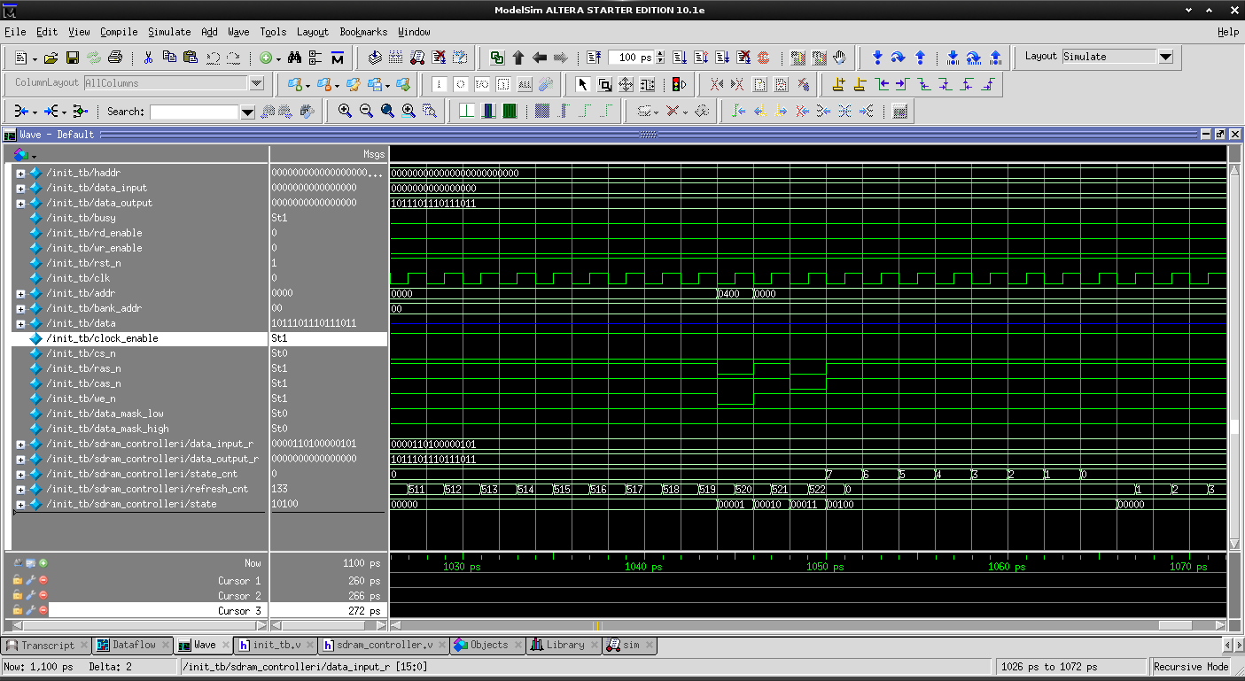
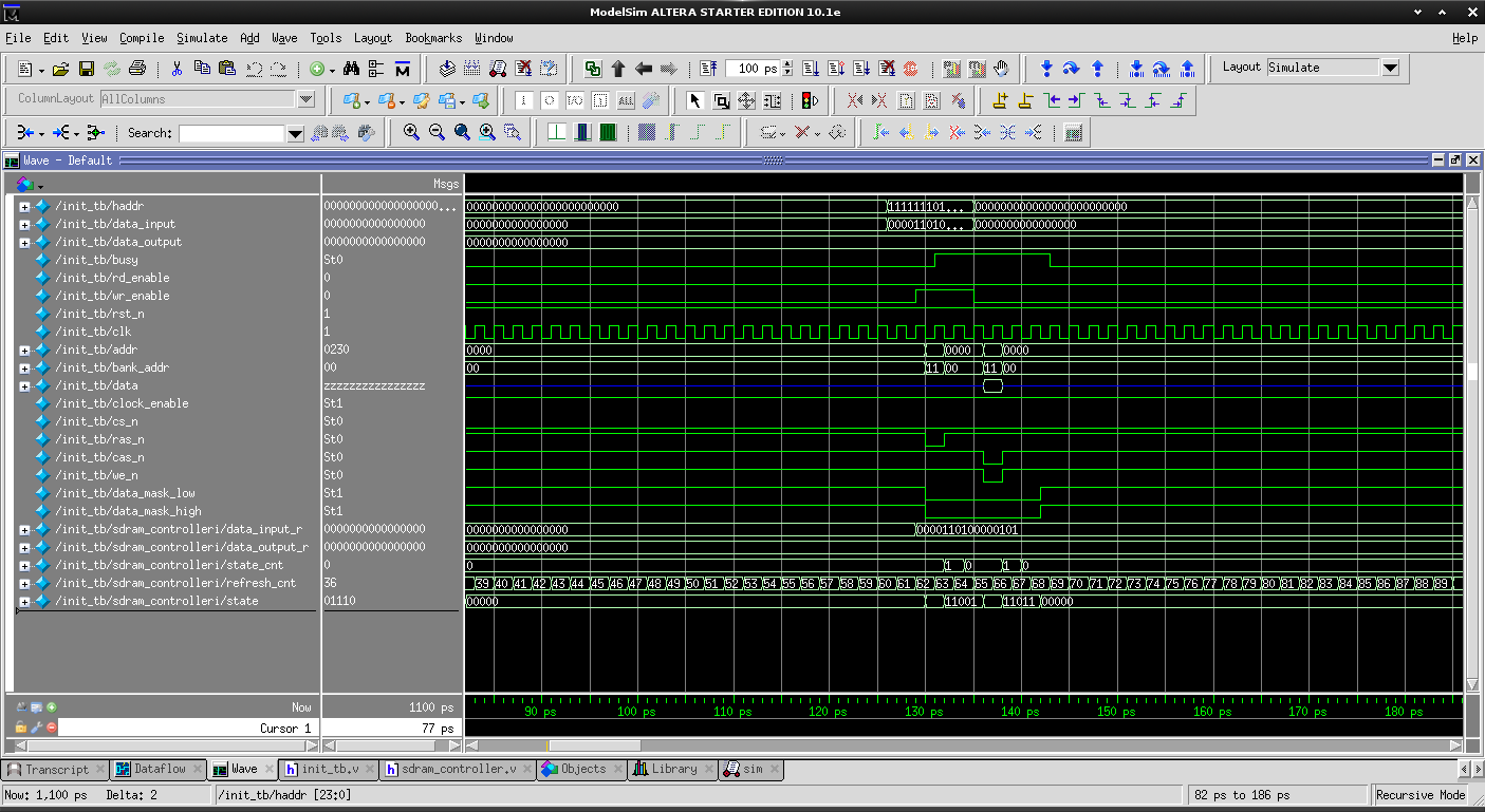
## Timings
# Initialization
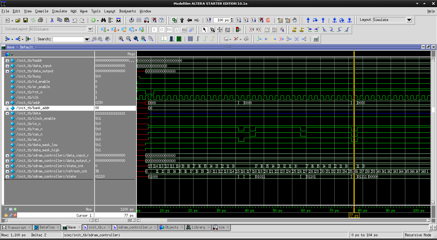
Initialization process showing:
- Precharge all banks
- 2 refresh cycles
- Mode programming
# Refresh
Refresh process showing:
- Precharge all banks
- Single Refresh
# Writes
Write operation showing:
- Bank Activation & Row Address Strobe
- Column Address Strobe with Auto Precharge set and Data on bus
# Reads
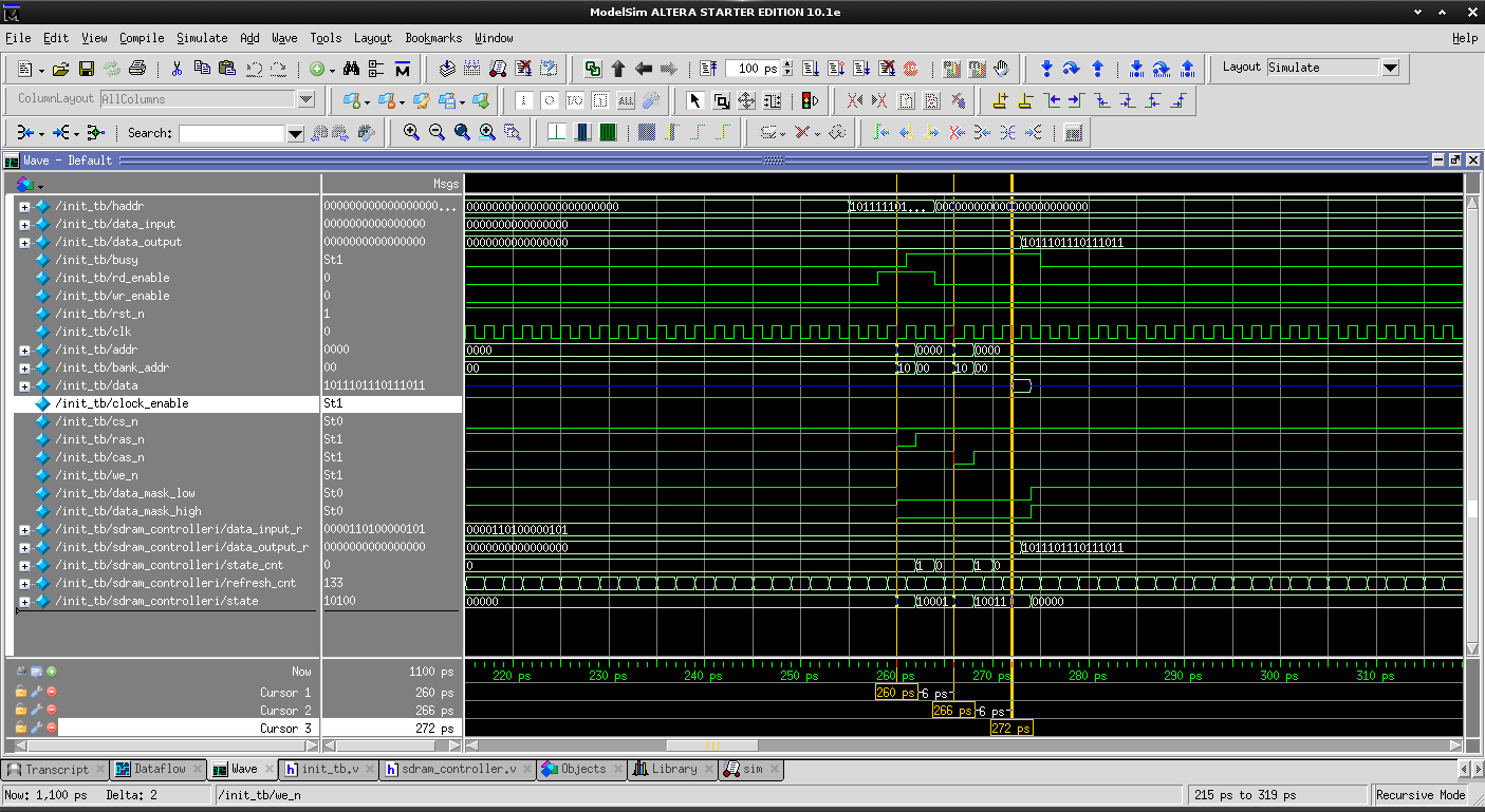
Read operation showing:
- Bank Activation & Row Address Strobe
- Column Address Strobe with Auto Precharge set
- Data on bus
## Test Application
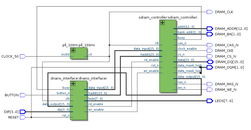
*Figure - test application block diagram*
The test application provides a simple user interface for testing the functionality
of the sdram controller.
Basics:
- The clock input should be 50Mhz (a pll multiplies it up to 100Mhz)
- One push button is used for `reset`
- A Second push button is used for `read` and `write`
- single click for `write`
- double click for `read`
- A 4-bit dip switch is used for inputting addresses and data
- Upon `reset` the read/write addresses are read from the dip switch
- When `writing` the dip switch is data is written to the sdram
- Address and data busses are greather than 4 bits, data is duplicated to fill the bus
- 8 LEDs are used to display the data read from the sdram. The data but is 16-bits, high and low bytes are alternated on the LEDs about every half second.
## Project Status/TODO
- [x] Compiles
- [x] Simulated `Init`
- [x] Simulated `Refresh`
- [x] Simulated `Read`
- [x] Simulated `Write`
- [x] Confirmed in De0 Nano
## Project Setup
This project has been developed with altera quartus II.
## License
BSD
## Further Reading
I didn't look at these when designing my controller. But it might be good to take a look at for ideas.
- http://hamsterworks.co.nz/mediawiki/index.php/Simple_SDRAM_Controller - featured on hackaday
- http://ladybug.xs4all.nl/arlet/fpga/source/sdram.v - Arlet's implementation from a comment on the hackaday article
================================================
FILE: rtl/dnano_interface.v
================================================
/* De0 Nano interface for testing sdram controller
* Handles interpreting buttons and switches
* to talk to the sdram controller.
*/
module dnano_interface (
/* Human Interface */
button_n, dip, leds,
/* Controller Interface */
haddr, // RW-FIFO- data1
busy, // RW-FIFO- full
wr_enable, // WR-FIFO- write
wr_data, // WR-FIFO- data2
rd_enable, //RO-FIFO- write
rd_data, //RI-FIFO- data
rd_rdy, // RI-FIFO-~empty
rd_ack, // RI-FIFO- read
/* basics */
rst_n, clk
);
parameter HADDR_WIDTH = 24;
// @ 1mhz 19bit (512K) is about 1/2 second
// @ 100mhz 26bit (64M) is about 1/2 second
localparam DOUBlE_CLICK_WAIT = 19;
localparam LED_BLINK = 20;
input button_n;
input [3:0] dip;
output [7:0] leds;
output [HADDR_WIDTH-1:0] haddr;
output [15:0] wr_data;
input [15:0] rd_data;
input busy;
output rd_enable;
input rd_rdy;
output rd_ack;
output wr_enable;
input rst_n;
input clk;
wire [15:0] wr_data;
reg [15:0] rd_data_r;
reg [LED_BLINK-1:0] led_cnt;
wire [7:0] leds;
wire wr_enable;
reg rd_ack_r;
wire dbl_clck_rst_n;
// When to reset the double click output
// we want to reset after we know the sdram is busy
// busy | rst_n
// 0 0 - reset is on (be-low )
// 0 1 - reset is off (be high)
// 1 0 - busy + reset (be-low)
// 1 1 - busy is on (be-low)
assign dbl_clck_rst_n = rst_n & ~busy;
// expand the dip data from 4 to 16 bits
assign wr_data = {dip, dip, ~dip, ~dip};
// toggle leds between sdram msb and lsb
assign leds = led_cnt[LED_BLINK-1] ? rd_data_r[15:8] : rd_data_r[7:0];
assign haddr = {(HADDR_WIDTH/4){dip}};
assign rd_ack = rd_ack_r;
// handle led counter should just loop every half second
always @ (posedge clk)
if (~rst_n)
led_cnt <= {LED_BLINK{1'b0}};
else
led_cnt <= led_cnt + 1'b1;
always @ (posedge clk)
if (~rst_n)
begin
rd_data_r <= 16'b0;
rd_ack_r <= 1'b0;
end
else
begin
rd_ack_r <= rd_rdy;
if (rd_rdy)
rd_data_r <= rd_data;
else
rd_data_r <= rd_data_r;
end
double_click #(.WAIT_WIDTH(DOUBlE_CLICK_WAIT)) double_clicki (
.button (~button_n),
.single (wr_enable),
.double (rd_enable),
.clk (clk),
.rst_n (dbl_clck_rst_n)
);
endmodule
================================================
FILE: rtl/double_click.v
================================================
/* Input is a button
* Detect if the button is double clicked or single clicked in
* a time interval. Outputs are maintained until reset.
*/
module double_click (
button,
single, double,
clk, rst_n
);
parameter WAIT_WIDTH = 19;
input button;
output single, double;
input clk, rst_n;
reg btn_now, btn_last, collect;
reg [2:0] click_cnt;
reg [WAIT_WIDTH-1:0] dbl_click_cnt;
// if we are done counting and we have 1 click its single, else double
assign single = (!dbl_click_cnt & (click_cnt == 3'b001)) ? 1'b1 : 1'b0;
assign double = (!dbl_click_cnt & (click_cnt != 3'b001)) ? 1'b1 : 1'b0;
// detect button down vs button up
wire btn_down = btn_now & ~btn_last;
//wire btn_up = ~btn_now & btn_last;
always @ (negedge clk)
if (~rst_n)
{ btn_last, btn_now } <= 2'b00;
else
{ btn_last, btn_now } <= { btn_now, button };
// start down counter and count clicks
always @ (posedge clk)
if (~rst_n)
begin
click_cnt <= 3'd0;
dbl_click_cnt <= {WAIT_WIDTH{1'b1}};
collect <= 1'b0;
end
else
begin
if (collect & (dbl_click_cnt != {WAIT_WIDTH{1'b0}}))
dbl_click_cnt <= dbl_click_cnt - 1'b1;
else
dbl_click_cnt <= dbl_click_cnt;
if (btn_down)
begin
collect <= 1'b1;
click_cnt <= click_cnt + 1'b1;
end
else
begin
collect <= collect;
click_cnt <= click_cnt;
end
end
endmodule
================================================
FILE: rtl/fifo.v
================================================
/*
* This is a 2 clock fifo used for transferring data between
* clock domains.
*
* I assume here that the output (read) clock is >5X slower than the
* input (write) clock.
*
* Also, the fifo is just 1 word deep.
*
* Changes
* - 2015-07-03 issue when writing from low speed clock, empty_n goes
* high and stays high. The reader side will see and read, but
* after complete empty_n is still high. It will continue
* to read until empty_n is lowered based on the write side
* clock.
* The empty_n should go low once the reader reads.
*
*/
module fifo (
// Write side
wr_clk,
wr_data,
wr,
full, // means don't write any more
// Read side
rd_data,
rd_clk,
rd,
empty_n, // also means we can read
rst_n
);
parameter BUS_WIDTH = 16;
input [BUS_WIDTH-1:0] wr_data;
input wr_clk;
input wr;
output full; // Low-Means in side can write
output [BUS_WIDTH-1:0] rd_data;
input rd_clk;
input rd;
output empty_n; // High-Means out side can read
input rst_n;
reg [BUS_WIDTH-1:0] wr_data_r;
reg [BUS_WIDTH-1:0] rd_data;
/*
* these reg sets span accross 2 clock domtains
* CLK WR | CLK RD
* [wr_r] ------------------> | -> [wr_syn1] -> [wr_syn2] -\
* <- [wr_ack2] <- [wr_ack1] | ---------------------------/
* ^^^^^^^^^^ |
* Set wr_r when we get a wr | increment counter when we get
* Clr wr when we get wr_ack2 | wr_syn2, and syncronize data
*
*/
reg wr_r, wr_syn1, wr_syn2, wr_ack1, wr_ack2;
reg rd_r, rd_syn1, rd_syn2, rd_ack1, rd_ack2;
reg wr_fifo_cnt;
reg rd_fifo_cnt;
assign full = wr_fifo_cnt == 1'b1;
assign empty_n = rd_fifo_cnt == 1'b1;
always @ (posedge rd_clk)
if (~rst_n)
begin
rd_fifo_cnt <= 1'b0;
{rd_ack2, rd_ack1} <= 2'b00;
{wr_syn2, wr_syn1} <= 2'b00;
end
else
begin
{rd_ack2, rd_ack1} <= {rd_ack1, rd_syn2};
{wr_syn2, wr_syn1} <= {wr_syn1, wr_r};
if (rd)
rd_r <= 1'b1;
else if (rd_ack2)
rd_r <= 1'b0;
if (rd)
rd_fifo_cnt <= 1'b0;
if ({wr_syn2, wr_syn1} == 2'b01) // if we want to just do increment 1 time, we can check posedge
rd_fifo_cnt <= 1'b1;
if (wr_syn2)
rd_data <= wr_data_r;
end
always @ (posedge wr_clk)
if (~rst_n)
begin
wr_fifo_cnt <= 1'b0;
{rd_syn2, rd_syn1} <= 2'b00;
{wr_ack2, wr_ack1} <= 2'b00;
end
else
begin
{wr_ack2, wr_ack1} <= {wr_ack1, wr_syn2};
{rd_syn2, rd_syn1} <= {rd_syn1, rd_r};
if (wr)
wr_r <= 1'b1;
if (wr_ack2)
wr_r <= 1'b0;
if (wr)
wr_fifo_cnt <= 1'b1;
if ({rd_syn2, rd_syn1} == 2'b01)
wr_fifo_cnt <= 1'b0;
// register write data on write
if (wr)
wr_data_r <= wr_data;
end
endmodule
================================================
FILE: rtl/sdram_controller.v
================================================
/**
* simple controller for ISSI IS42S16160G-7 SDRAM found in De0 Nano
* 16Mbit x 16 data bit bus (32 megabytes)
* Default options
* 133Mhz
* CAS 3
*
* Very simple host interface
* * No burst support
* * haddr - address for reading and wriging 16 bits of data
* * data_input - data for writing, latched in when wr_enable is highz0
* * data_output - data for reading, comes available sometime
* *few clocks* after rd_enable and address is presented on bus
* * rst_n - start init ram process
* * rd_enable - read enable, on clk posedge haddr will be latched in,
* after *few clocks* data will be available on the data_output port
* * wr_enable - write enable, on clk posedge haddr and data_input will
* be latched in, after *few clocks* data will be written to sdram
*
* Theory
* This simple host interface has a busy signal to tell you when you are
* not able to issue commands.
*/
module sdram_controller (
/* HOST INTERFACE */
wr_addr,
wr_data,
wr_enable,
rd_addr,
rd_data,
rd_ready,
rd_enable,
busy, rst_n, clk,
/* SDRAM SIDE */
addr, bank_addr, data, clock_enable, cs_n, ras_n, cas_n, we_n,
data_mask_low, data_mask_high
);
/* Internal Parameters */
parameter ROW_WIDTH = 13;
parameter COL_WIDTH = 9;
parameter BANK_WIDTH = 2;
parameter SDRADDR_WIDTH = ROW_WIDTH > COL_WIDTH ? ROW_WIDTH : COL_WIDTH;
parameter HADDR_WIDTH = BANK_WIDTH + ROW_WIDTH + COL_WIDTH;
parameter CLK_FREQUENCY = 133; // Mhz
parameter REFRESH_TIME = 32; // ms (how often we need to refresh)
parameter REFRESH_COUNT = 8192; // cycles (how many refreshes required per refresh time)
// clk / refresh = clk / sec
// , sec / refbatch
// , ref / refbatch
localparam CYCLES_BETWEEN_REFRESH = ( CLK_FREQUENCY
* 1_000
* REFRESH_TIME
) / REFRESH_COUNT;
// STATES - State
localparam IDLE = 5'b00000;
localparam INIT_NOP1 = 5'b01000,
INIT_PRE1 = 5'b01001,
INIT_NOP1_1=5'b00101,
INIT_REF1 = 5'b01010,
INIT_NOP2 = 5'b01011,
INIT_REF2 = 5'b01100,
INIT_NOP3 = 5'b01101,
INIT_LOAD = 5'b01110,
INIT_NOP4 = 5'b01111;
localparam REF_PRE = 5'b00001,
REF_NOP1 = 5'b00010,
REF_REF = 5'b00011,
REF_NOP2 = 5'b00100;
localparam READ_ACT = 5'b10000,
READ_NOP1 = 5'b10001,
READ_CAS = 5'b10010,
READ_NOP2 = 5'b10011,
READ_READ = 5'b10100;
localparam WRIT_ACT = 5'b11000,
WRIT_NOP1 = 5'b11001,
WRIT_CAS = 5'b11010,
WRIT_NOP2 = 5'b11011;
// Commands CCRCWBBA
// ESSSE100
localparam CMD_PALL = 8'b10010001,
CMD_REF = 8'b10001000,
CMD_NOP = 8'b10111000,
CMD_MRS = 8'b1000000x,
CMD_BACT = 8'b10011xxx,
CMD_READ = 8'b10101xx1,
CMD_WRIT = 8'b10100xx1;
/* Interface Definition */
/* HOST INTERFACE */
input [HADDR_WIDTH-1:0] wr_addr;
input [15:0] wr_data;
input wr_enable;
input [HADDR_WIDTH-1:0] rd_addr;
output [15:0] rd_data;
input rd_enable;
output rd_ready;
output busy;
input rst_n;
input clk;
/* SDRAM SIDE */
output [SDRADDR_WIDTH-1:0] addr;
output [BANK_WIDTH-1:0] bank_addr;
inout [15:0] data;
output clock_enable;
output cs_n;
output ras_n;
output cas_n;
output we_n;
output data_mask_low;
output data_mask_high;
/* I/O Registers */
reg [HADDR_WIDTH-1:0] haddr_r;
reg [15:0] wr_data_r;
reg [15:0] rd_data_r;
reg busy;
reg data_mask_low_r;
reg data_mask_high_r;
reg [SDRADDR_WIDTH-1:0] addr_r;
reg [BANK_WIDTH-1:0] bank_addr_r;
reg rd_ready_r;
wire [15:0] data_output;
wire data_mask_low, data_mask_high;
assign data_mask_high = data_mask_high_r;
assign data_mask_low = data_mask_low_r;
assign rd_data = rd_data_r;
/* Internal Wiring */
reg [3:0] state_cnt;
reg [9:0] refresh_cnt;
reg [7:0] command;
reg [4:0] state;
// TODO output addr[6:4] when programming mode register
reg [7:0] command_nxt;
reg [3:0] state_cnt_nxt;
reg [4:0] next;
assign {clock_enable, cs_n, ras_n, cas_n, we_n} = command[7:3];
// state[4] will be set if mode is read/write
assign bank_addr = (state[4]) ? bank_addr_r : command[2:1];
assign addr = (state[4] | state == INIT_LOAD) ? addr_r : { {SDRADDR_WIDTH-11{1'b0}}, command[0], 10'd0 };
assign data = (state == WRIT_CAS) ? wr_data_r : 16'bz;
assign rd_ready = rd_ready_r;
// HOST INTERFACE
// all registered on posedge
always @ (posedge clk)
if (~rst_n)
begin
state <= INIT_NOP1;
command <= CMD_NOP;
state_cnt <= 4'hf;
haddr_r <= {HADDR_WIDTH{1'b0}};
wr_data_r <= 16'b0;
rd_data_r <= 16'b0;
busy <= 1'b0;
end
else
begin
state <= next;
command <= command_nxt;
if (!state_cnt)
state_cnt <= state_cnt_nxt;
else
state_cnt <= state_cnt - 1'b1;
if (wr_enable)
wr_data_r <= wr_data;
if (state == READ_READ)
begin
rd_data_r <= data;
rd_ready_r <= 1'b1;
end
else
rd_ready_r <= 1'b0;
busy <= state[4];
if (rd_enable)
haddr_r <= rd_addr;
else if (wr_enable)
haddr_r <= wr_addr;
end
// Handle refresh counter
always @ (posedge clk)
if (~rst_n)
refresh_cnt <= 10'b0;
else
if (state == REF_NOP2)
refresh_cnt <= 10'b0;
else
refresh_cnt <= refresh_cnt + 1'b1;
/* Handle logic for sending addresses to SDRAM based on current state*/
always @*
begin
if (state[4])
{data_mask_low_r, data_mask_high_r} = 2'b00;
else
{data_mask_low_r, data_mask_high_r} = 2'b11;
bank_addr_r = 2'b00;
addr_r = {SDRADDR_WIDTH{1'b0}};
if (state == READ_ACT | state == WRIT_ACT)
begin
bank_addr_r = haddr_r[HADDR_WIDTH-1:HADDR_WIDTH-(BANK_WIDTH)];
addr_r = haddr_r[HADDR_WIDTH-(BANK_WIDTH+1):HADDR_WIDTH-(BANK_WIDTH+ROW_WIDTH)];
end
else if (state == READ_CAS | state == WRIT_CAS)
begin
// Send Column Address
// Set bank to bank to precharge
bank_addr_r = haddr_r[HADDR_WIDTH-1:HADDR_WIDTH-(BANK_WIDTH)];
// Examples for math
// BANK ROW COL
// HADDR_WIDTH 2 + 13 + 9 = 24
// SDRADDR_WIDTH 13
// Set CAS address to:
// 0s,
// 1 (A10 is always for auto precharge),
// 0s,
// column address
addr_r = {
{SDRADDR_WIDTH-(11){1'b0}},
1'b1, /* A10 */
{10-COL_WIDTH{1'b0}},
haddr_r[COL_WIDTH-1:0]
};
end
else if (state == INIT_LOAD)
begin
// Program mode register during load cycle
// B C SB
// R A EUR
// S S-3Q ST
// T 654L210
addr_r = {{SDRADDR_WIDTH-10{1'b0}}, 10'b1000110000};
end
end
// Next state logic
always @*
begin
state_cnt_nxt = 4'd0;
command_nxt = CMD_NOP;
if (state == IDLE)
// Monitor for refresh or hold
if (refresh_cnt >= CYCLES_BETWEEN_REFRESH)
begin
next = REF_PRE;
command_nxt = CMD_PALL;
end
else if (rd_enable)
begin
next = READ_ACT;
command_nxt = CMD_BACT;
end
else if (wr_enable)
begin
next = WRIT_ACT;
command_nxt = CMD_BACT;
end
else
begin
// HOLD
next = IDLE;
end
else
if (!state_cnt)
case (state)
// INIT ENGINE
INIT_NOP1:
begin
next = INIT_PRE1;
command_nxt = CMD_PALL;
end
INIT_PRE1:
begin
next = INIT_NOP1_1;
end
INIT_NOP1_1:
begin
next = INIT_REF1;
command_nxt = CMD_REF;
end
INIT_REF1:
begin
next = INIT_NOP2;
state_cnt_nxt = 4'd7;
end
INIT_NOP2:
begin
next = INIT_REF2;
command_nxt = CMD_REF;
end
INIT_REF2:
begin
next = INIT_NOP3;
state_cnt_nxt = 4'd7;
end
INIT_NOP3:
begin
next = INIT_LOAD;
command_nxt = CMD_MRS;
end
INIT_LOAD:
begin
next = INIT_NOP4;
state_cnt_nxt = 4'd1;
end
// INIT_NOP4: default - IDLE
// REFRESH
REF_PRE:
begin
next = REF_NOP1;
end
REF_NOP1:
begin
next = REF_REF;
command_nxt = CMD_REF;
end
REF_REF:
begin
next = REF_NOP2;
state_cnt_nxt = 4'd7;
end
// REF_NOP2: default - IDLE
// WRITE
WRIT_ACT:
begin
next = WRIT_NOP1;
state_cnt_nxt = 4'd1;
end
WRIT_NOP1:
begin
next = WRIT_CAS;
command_nxt = CMD_WRIT;
end
WRIT_CAS:
begin
next = WRIT_NOP2;
state_cnt_nxt = 4'd1;
end
// WRIT_NOP2: default - IDLE
// READ
READ_ACT:
begin
next = READ_NOP1;
state_cnt_nxt = 4'd1;
end
READ_NOP1:
begin
next = READ_CAS;
command_nxt = CMD_READ;
end
READ_CAS:
begin
next = READ_NOP2;
state_cnt_nxt = 4'd1;
end
READ_NOP2:
begin
next = READ_READ;
end
// READ_READ: default - IDLE
default:
begin
next = IDLE;
end
endcase
else
begin
// Counter Not Reached - HOLD
next = state;
command_nxt = command;
end
end
endmodule
================================================
FILE: rtl/toplevel.sdc
================================================
create_clock -period "20ns" CLOCK_50
derive_pll_clocks
derive_clock_uncertainty
================================================
FILE: rtl/toplevel.v
================================================
//////////////////////////////////////////////////////////////////////
//
// toplevel for dram controller de0 nano board
//
//////////////////////////////////////////////////////////////////////
//
// This source file may be used and distributed without
// restriction provided that this copyright statement is not
// removed from the file and that any derivative work contains
// the original copyright notice and the associated disclaimer.
//
// This source file is free software; you can redistribute it
// and/or modify it under the terms of the GNU Lesser General
// Public License as published by the Free Software Foundation;
// either version 2.1 of the License, or (at your option) any
// later version.
//
// This source is distributed in the hope that it will be
// useful, but WITHOUT ANY WARRANTY; without even the implied
// warranty of MERCHANTABILITY or FITNESS FOR A PARTICULAR
// PURPOSE. See the GNU Lesser General Public License for more
// details.
//
// You should have received a copy of the GNU Lesser General
// Public License along with this source; if not, download it
// from http://www.opencores.org/lgpl.shtml
//
//////////////////////////////////////////////////////////////////////
module toplevel (
input sys_clk_pad_i,
input rst_n_pad_i,
input btn_n_pad_i,
output [1:0] sdram_ba_pad_o,
output [12:0] sdram_a_pad_o,
output sdram_cs_n_pad_o,
output sdram_ras_pad_o,
output sdram_cas_pad_o,
output sdram_we_pad_o,
inout [15:0] sdram_dq_pad_io,
output [1:0] sdram_dqm_pad_o,
output sdram_cke_pad_o,
output sdram_clk_pad_o,
inout [7:0] gpio0_io, /* LEDs */
input [3:0] gpio1_i /* DIPs */
);
wire clk100m;
wire clk1m;
assign sdram_clk_pad_o = clk100m;
// PLLs
pll_100m pll_100mi (
.inclk0 (sys_clk_pad_i),
.c0 (clk100m)
);
pll_1m pll_1mi (
.inclk0 (sys_clk_pad_i),
.c0 (clk1m)
);
// Cross Clock FIFOs
/* Address 24-bit and 16-bit Data transfers from in:1m out:100m */
/* 1 mhz side wires */
wire [39:0] wr_fifo;
wire wr_enable; /* wr_enable ] <-> [ wr : wr_enable to push fifo */
wire wr_full; /* wr_full ] <-> [ full : signal that we are full */
/* 100mhz side wires */
wire [39:0] wro_fifo;
wire ctrl_busy; /* rd ] <-> [ busy : pop fifo when ctrl not busy */
wire ctrl_wr_enable; /* .empty_n-wr_enable : signal ctrl data is ready */
fifo #(.BUS_WIDTH(40)) wr_fifoi (
.wr_clk (clk1m),
.rd_clk (clk100m),
.wr_data (wr_fifo),
.rd_data (wro_fifo),
.rd (ctrl_busy),
.wr (wr_enable),
.full (wr_full),
.empty_n (ctrl_wr_enable),
.rst_n (rst_n_pad_i)
);
/* Address 24-bit transfers from in:1m out:100m */
/* 1 mhz side wires */
wire rd_enable; /* rd_enable -wr : rd_enable to push rd addr to fifo */
wire rdaddr_full;/* rdaddr_full-full : signal we cannot read more */
/* 100mhz side wires */
wire [23:0] rdao_fifo;
wire ctrl_rd_enable; /* empty_n - rd_enable: signal ctrl addr ready */
fifo #(.BUS_WIDTH(24)) rdaddr_fifoi (
.wr_clk (clk1m),
.rd_clk (clk100m),
.wr_data (wr_fifo[39:16]),
.rd_data (rdao_fifo),
.rd (ctrl_busy),
.wr (rd_enable),
.full (rdaddr_full),
.empty_n (ctrl_rd_enable),
.rst_n (rst_n_pad_i)
);
/* 100mhz side wires */
wire [15:0] rddo_fifo;
wire ctrl_rd_ready; /* wr - rd_ready - push data from dram to fifo */
/* 1mhz side wires */
wire [15:0] rddata_fifo;
wire rd_ready; /* rd_ready-empty_n- signal interface data ready */
wire rd_ack; /* rd_ack - rd - pop fifo after data read */
/* Incoming 16-bit data transfers from in:100m out:1m */
fifo #(.BUS_WIDTH(16)) rddata_fifoi (
.wr_clk (clk100m),
.rd_clk (clk1m),
.wr_data (rddo_fifo),
.rd_data (rddata_fifo),
.rd (rd_ack),
.wr (ctrl_rd_ready),
.full (),
.empty_n (rd_ready),
.rst_n (rst_n_pad_i)
);
/* SDRAM */
sdram_controller sdram_controlleri (
/* HOST INTERFACE */
.wr_addr (wro_fifo[39:16]),
.wr_data (wro_fifo[15:0]),
.wr_enable (ctrl_wr_enable),
.rd_addr (rdao_fifo),
.rd_data (rddo_fifo),
.rd_ready (ctrl_rd_ready),
.rd_enable (ctrl_rd_enable),
.busy (ctrl_busy),
.rst_n (rst_n_pad_i),
.clk (clk100m),
/* SDRAM SIDE */
.addr (sdram_a_pad_o),
.bank_addr (sdram_ba_pad_o),
.data (sdram_dq_pad_io),
.clock_enable (sdram_cke_pad_o),
.cs_n (sdram_cs_n_pad_o),
.ras_n (sdram_ras_pad_o),
.cas_n (sdram_cas_pad_o),
.we_n (sdram_we_pad_o),
.data_mask_low (sdram_dqm_pad_o[0]),
.data_mask_high(sdram_dqm_pad_o[1])
);
wire busy;
assign busy = wr_full | rdaddr_full;
dnano_interface #(.HADDR_WIDTH(24)) dnano_interfacei (
/* Human Interface */
.button_n (btn_n_pad_i),
.dip (gpio1_i),
.leds (gpio0_io),
/* Controller Interface */
.haddr (wr_fifo[39:16]),// RW-FIFO- data1
.busy (busy), // RW-FIFO- full
.wr_enable (wr_enable), // WR-FIFO- write
.wr_data (wr_fifo[15:00]),// WR-FIFO- data2
.rd_enable (rd_enable), // RO-FIFO- write
.rd_data (rddata_fifo), // RI-FIFO- data
.rd_rdy (rd_ready), // RI-FIFO-~empty
.rd_ack (rd_ack), // RI-FIFO- read
/* basics */
.rst_n (rst_n_pad_i),
.clk (clk1m)
);
endmodule // toplevel
gitextract__b946yeo/
├── .gitignore
├── bench/
│ ├── double_click_tb.v
│ ├── fifo_tb.v
│ └── sdram_controller_tb.v
├── data/
│ ├── de0_nano.sdc
│ ├── options.tcl
│ └── pinmap.tcl
├── dram_controller.core
├── dram_controller.system
├── quartus/
│ ├── dram_controller.qpf
│ ├── dram_controller.qsf
│ ├── pll_100m.v
│ ├── pll_1m.v
│ └── vsim-wave.do
├── readme.md
└── rtl/
├── dnano_interface.v
├── double_click.v
├── fifo.v
├── sdram_controller.v
├── toplevel.sdc
└── toplevel.v
Condensed preview — 21 files, each showing path, character count, and a content snippet. Download the .json file or copy for the full structured content (93K chars).
[
  {
    "path": ".gitignore",
    "chars": 142,
    "preview": "fusesoc.log\n\n*.bak\n*.rpt\n*.qws\n*.bmp\nPLLJ_PLLSPE_INFO.txt\n\nwork/\ngreybox_tmp/\nsimulation/\ndb/\nincremental_db/\noutput_fil"
  },
  {
    "path": "bench/double_click_tb.v",
    "chars": 823,
    "preview": "/**\n * Test bench for double click detector module, simulates\n *  - Reset\n *  - 1-Click\n *  - 2-Click - expect 2 -click\n"
  },
  {
    "path": "bench/fifo_tb.v",
    "chars": 1194,
    "preview": "/**\n * Test bentch for fifo's\n *  1. fifo fast write read slow\n *  2. fifo write flow read fast\n *  3. fifo slight diffe"
  },
  {
    "path": "bench/sdram_controller_tb.v",
    "chars": 1722,
    "preview": "/**\n * Testbench for sdram_controller modules, simulates:\n *  - Iinit\n *  - Write\n *  - Read\n */\nmodule sdram_controller"
  },
  {
    "path": "data/de0_nano.sdc",
    "chars": 392,
    "preview": "# Main system clock (50 Mhz)\ncreate_clock -name \"sys_clk_pad_i\" -period 20.000ns [get_ports {sys_clk_pad_i}]\n\n# Automati"
  },
  {
    "path": "data/options.tcl",
    "chars": 0,
    "preview": ""
  },
  {
    "path": "data/pinmap.tcl",
    "chars": 10232,
    "preview": "#\n# Clock / Reset\n#\nset_location_assignment PIN_J15 -to rst_n_pad_i\nset_instance_assignment -name IO_STANDARD \"3.3-V LVT"
  },
  {
    "path": "dram_controller.core",
    "chars": 818,
    "preview": "CAPI=1\n[main]\ndescription = \"Stafford's toy dram controller for de0 nano\"\nsimulators = icarus\n\n[fileset rtl_files]\nfiles"
  },
  {
    "path": "dram_controller.system",
    "chars": 280,
    "preview": "SAPI=1\n[main]\nname = dram_controller\ndescription = \"Stafford toy dram controller for de0 Nano\"\n\nbackend = quartus\n\n[quar"
  },
  {
    "path": "quartus/dram_controller.qpf",
    "chars": 1326,
    "preview": "# -------------------------------------------------------------------------- #\n#\n# Copyright (C) 1991-2015 Altera Corpor"
  },
  {
    "path": "quartus/dram_controller.qsf",
    "chars": 12283,
    "preview": "# -------------------------------------------------------------------------- #\n#\n# Copyright (C) 1991-2015 Altera Corpor"
  },
  {
    "path": "quartus/pll_100m.v",
    "chars": 14465,
    "preview": "// megafunction wizard: %ALTPLL%\n// GENERATION: STANDARD\n// VERSION: WM1.0\n// MODULE: altpll \n\n// ======================"
  },
  {
    "path": "quartus/pll_1m.v",
    "chars": 14380,
    "preview": "// megafunction wizard: %ALTPLL%\n// GENERATION: STANDARD\n// VERSION: WM1.0\n// MODULE: altpll \n\n// ======================"
  },
  {
    "path": "quartus/vsim-wave.do",
    "chars": 1599,
    "preview": "onerror {resume}\nquietly WaveActivateNextPane {} 0\nadd wave -noupdate -radix binary /init_tb/haddr\nadd wave -noupdate /i"
  },
  {
    "path": "readme.md",
    "chars": 5018,
    "preview": "# _SDRAM Memory Controller_\n\n`CURRENT STATUS : stable`\n\nThis is a very a simple sdram controller which works on the De0 "
  },
  {
    "path": "rtl/dnano_interface.v",
    "chars": 2538,
    "preview": "/* De0 Nano interface for testing sdram controller \n * Handles interpreting buttons and switches \n * to talk to the sdra"
  },
  {
    "path": "rtl/double_click.v",
    "chars": 1365,
    "preview": "/* Input is a button \n * Detect if the button is double clicked or single clicked in \n * a time interval. Outputs are ma"
  },
  {
    "path": "rtl/fifo.v",
    "chars": 3117,
    "preview": "/*\n * This is a 2 clock fifo used for transferring data between\n * clock domains. \n * \n * I assume here that the output "
  },
  {
    "path": "rtl/sdram_controller.v",
    "chars": 10756,
    "preview": "/**\n * simple controller for ISSI IS42S16160G-7 SDRAM found in De0 Nano\n *  16Mbit x 16 data bit bus (32 megabytes)\n *  "
  },
  {
    "path": "rtl/toplevel.sdc",
    "chars": 80,
    "preview": "create_clock -period \"20ns\" CLOCK_50\nderive_pll_clocks\nderive_clock_uncertainty\n"
  },
  {
    "path": "rtl/toplevel.v",
    "chars": 5813,
    "preview": "//////////////////////////////////////////////////////////////////////\n//\n// toplevel for dram controller de0 nano board"
  }
]
About this extraction
This page contains the full source code of the stffrdhrn/sdram-controller GitHub repository, extracted and formatted as plain text for AI agents and large language models (LLMs). The extraction includes 21 files (86.3 KB), approximately 25.3k tokens. Use this with OpenClaw, Claude, ChatGPT, Cursor, Windsurf, or any other AI tool that accepts text input. You can copy the full output to your clipboard or download it as a .txt file.
Extracted by GitExtract — free GitHub repo to text converter for AI. Built by Nikandr Surkov.